Curve Tracer Applications


Kennlinienschreiber
Tektronix 576 Curve Tracer


This application note gives an overwiew about curve tracer measurements


(please, see also the instruction manual for measurement examples)

Resistor Curves


offen                Kurzschluss
High Ohm Resistor - Adapter with a open circuit                                                                      Low Ohm Resistor - Adapter with a short circuit


220 Ohm Carbon Resistor 


Horizontal Deflection Factor = 1V/Division
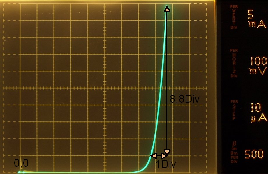
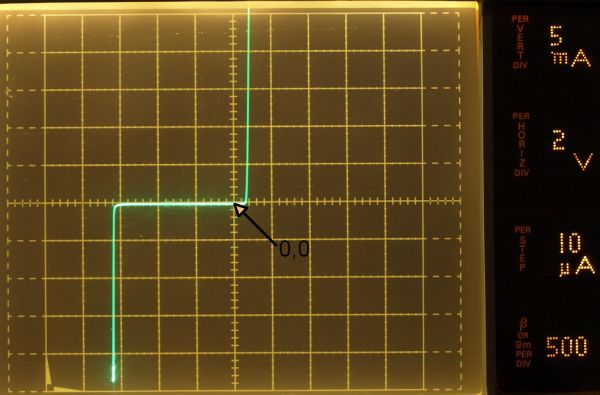
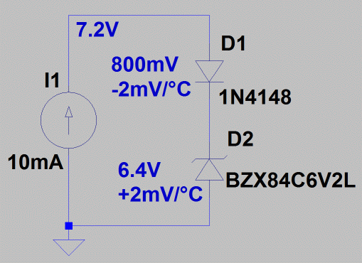
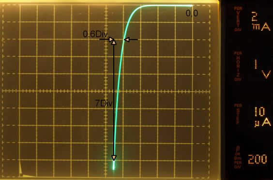
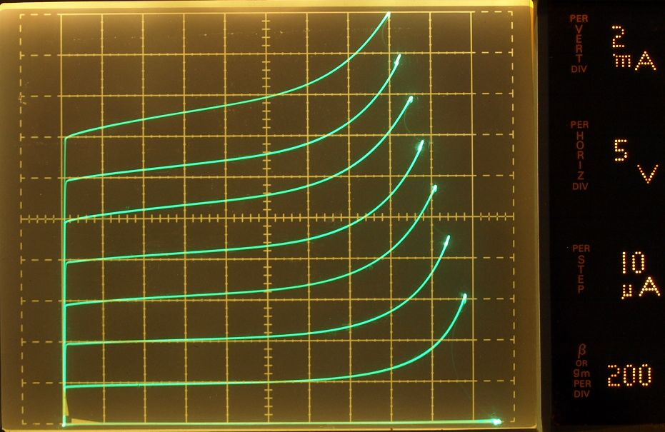
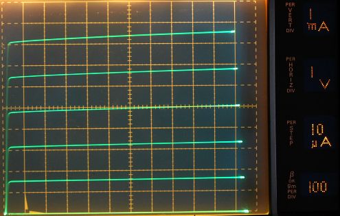
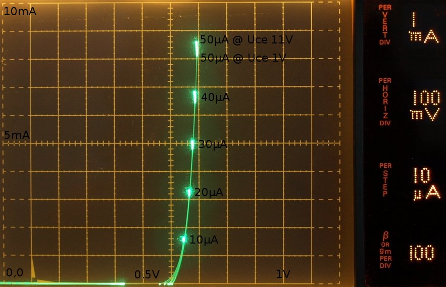
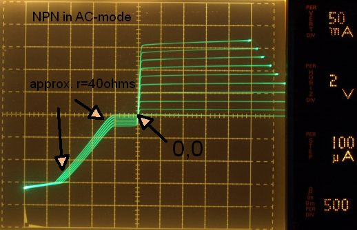
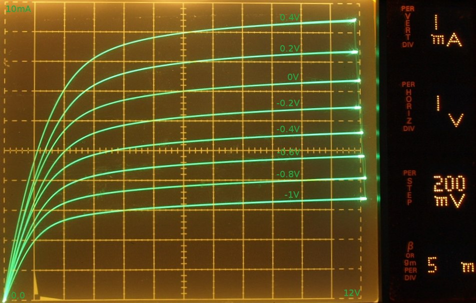
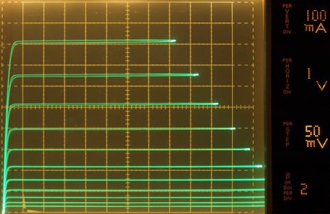
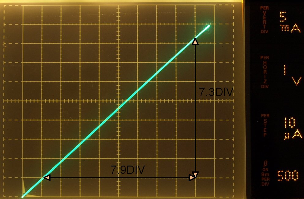
Vertical Deflection Factor = 5mA/Division

7.9DIV * 1V/DIV = 7.9V
7.3DIV * 5mA/DIV = 36.5mA
Resistance = 7.9V/36.5mA

Resistance = 216.4 Ohm
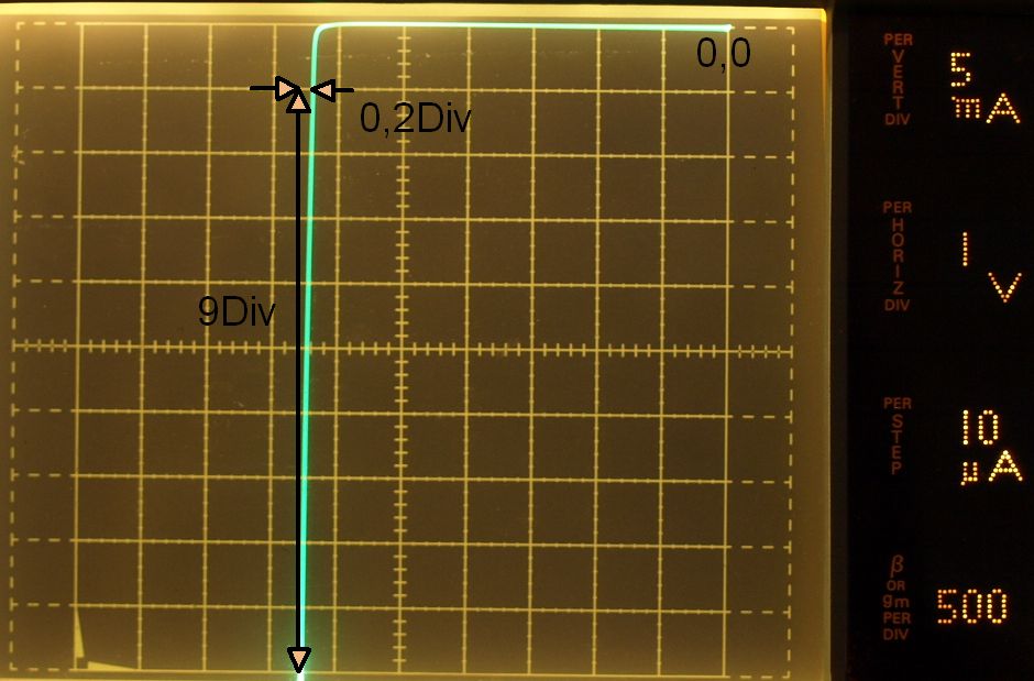
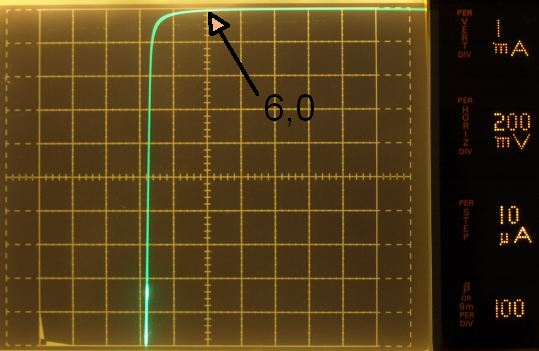
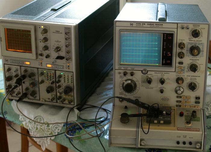
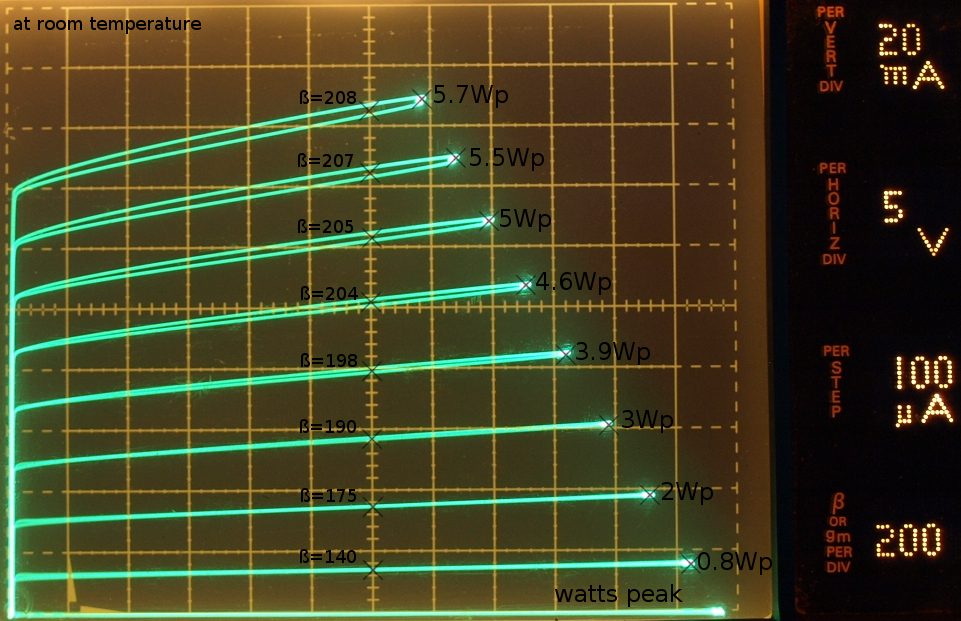
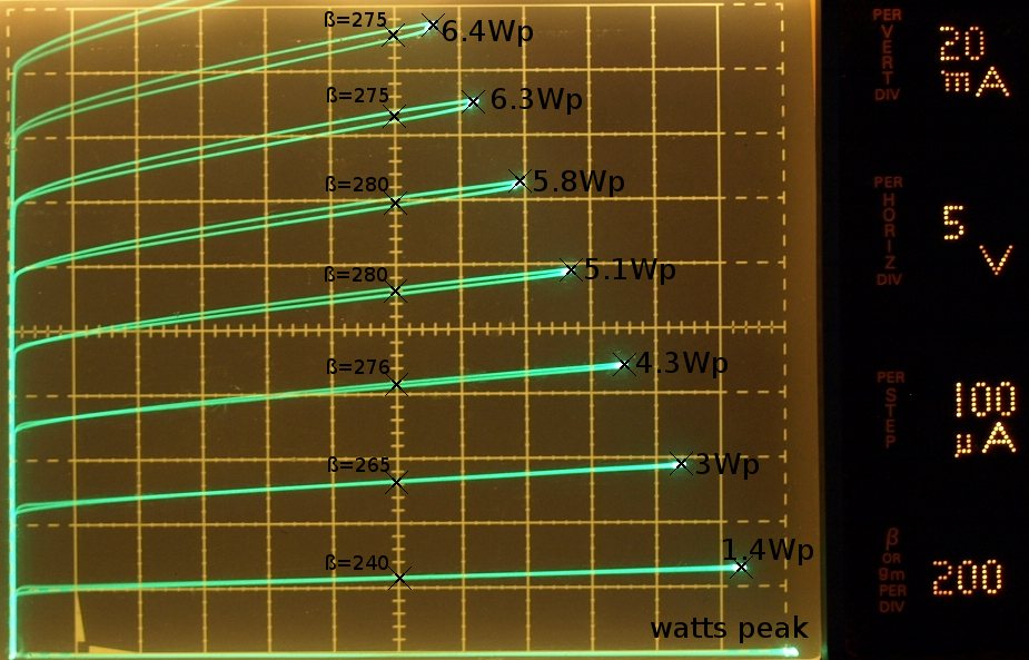
Applied Peak Power
hor.=9.7DIV and vert.=8.9DIV
hor.=9.3V and vert.=44.5mA
Peak Power = 414mW

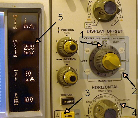
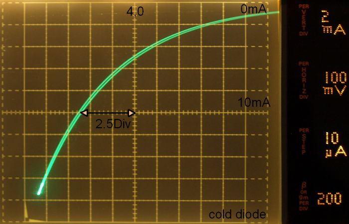
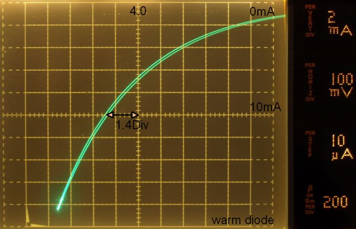
(note: use most top/bottom and right/left
graticules for delta measurement only when
CRT geometry is in accurate condition)
Resistors can be measured by reading the deflection, they can't be measured with high precision. The curve tracer shows larger nonlinearities easily. It's also a powerful tool for checking NTC and PTC resistors and other temperature or power dependend devices.


Zener Diode Curves

zenerdiode 6.2V
6.2 Volt Zener Diode


Forward biased zener diode (Curve Tracer set to NPN mode)


0,0 indicates zero voltage and zero current.
Diode starts with a very high resistance.
Approximately at 650mV diode starts with conducting to its low ohm area.
8.8Div * 5mA/Div = 44mA
1Div * 100mV/Div = 100mV
Differential resistance = 2.2 ohms
The current vs. voltage follows a curve with an exponential character
Derived differential resistance decreases with eponential character too.


Reversed biased zener diode (Curve Tracer set to PNP mode)

Approximately at 6.2 volt the diode starts conducting.
It's difficult to measure the differential resistance because of the steep slope.
differential slope = 0.2Div/9Div
differential resistance = 4.4 ohms
The 6.2V offset can be removed by a display offset mode, will show later.


Zener Diode AC-Mode Polarity


 6.2V zener diode in the curve tracer Polarity Switch AC-Mode

The AC mode allows a positive and negative going curve with in one diagram.  This mode set the zero voltage/current automatically to the center graticule.


6.2V Zener Diode Display Offset


With these settings the knee area of the 6.2V zener diode can be better observed.

1. Shift curve by 3 Divisions to the right side
2. Horizontal expansion by factor 10, 2V/Div goes to 200mV/Div
3. Push for indicating adjusted the 6,0 point
4. Unexpanded horizontal deflection still 2V/Div
5. Expanded horizontal deflection 200mV/Div appears on screen.


Note the 200mV/Div horizontal deflection.
The 6.0V/0mA point marked by the arrow.
The knee area can be better observed.
Consider this display offset advantage when using e.g. a 200V  zener diode


Describing this Display Offset Mode in a few words only is difficult. In pratice when using the curve tracer it is more easy than reading only.


6.2V Zener Diode Temperature Experiment - Forward Biased


Heating the diode environmental for a short moment with a lighter.


Forward biased 6.2V zener diode at room temperature


Forward biased 6.2V zener diode external heated

At the same 5mA current the foward voltage has been decreased  by heating the junction.

7.8Div * 100mV/Div = 780mV @ 5mA cold
7.6Div * 100mV/Div = 760mV @ 5mA warm

Difference caused by temperature rise = -20mV

A silicon junction has approximately a temperature coefficient of -2mV/°C
therefore the diode junction has been increased by approximately
(-20mV/-2mV) * °C = 10°C

The lighter increased the silicon junction temperature approximately by 10°C.

Directly observed on the CRT are these experiments very impressful like a good video, even touching by the hand will show clearly effects on the tracer.


6.2V Zener Diode Temperature Experiment - Reversed Biased


Reversed biased 6.2V Zener diode - diode at room temperature - display offset vertical 10 * expanded


Reversed biased 6.2V Zener diode - diode heated with the lighter - display offset vertical 10 * expanded

At the same 10mA current the diode voltage increase with temperature
(compare in forward direction diode voltage decreased with temperature)

By knowing the temperature rise the positive voltage coefficient could be calculated now.

When guessing the temperature increased by 10°C and the voltage increased by 0.2DIV (20mV), it can be said in reverse direction the zener diode voltage increase approximately with

+2mV/°C


A series connection of a forward biased silicon junction and a 6.2V zener diode can cancel out the overall temperature coefficient.
This cancelation method requires the knowledge for the best current value, because both diode TCs depending on applied current.
Driven by a current source this circuit method is called zener voltage reference.
There are Temperature Coefficient Compensated diodes and many ICs available operating on that method.


5.1V Zener Diode Temperature Experiment - Reversed Biased


A 5.1V zener diode will behaviour different from a 6.2V zener.


5.1V Zener diode reverse biased
7DIV*2mA/DIV=14mA
0.6DIV*1V/DIV=600mV

Differential Resistance = 600mV/14mA = 42 ohms

It is well known a 5.1V zener won't reach the lowest differential resistors of a 6.2V, which is a type with the lowest differential resistance.
Differential resistance decrease with increasing current.


Again using a lighter for increasing temperature.


Reversed biased 5.1V Zener diode - diode at room temperature - display offset vertical 10 * expanded


Reversed biased 5.1V Zener diode - diode heated with the lighter - display offset vertical 10 * expanded

At the same 10mA current the diode voltage decrease with temperature

The 5.1V zener diode type has an negative voltage temperature coefficient compared to a 6.2V zener, a 5.6V zener has a better TC somewhere between the 5.1V and 6.2V type.

Simplified said as single device 5.6V zeners are good in TC behaviour and 6.2V zeners are best in lowest differential resistance, all other voltages getting more worse compared to these both types.


Display Offset Settings when measuring the reversed 5.1V zener.


NPN 2N2219 Transistor Curves - Collector Current vs. Uce @ Ib steps


This is a  NPN 2N2219 transistor, marked with TFK, (could stand for a Telefunken)


This diagram uses the curve tracer step generator

Collector current vs. collector-emitter voltage for base current steps.


It is seen with increasing collector currents the differential resistance (Uce / Ic) decreases.
Current gain (Ic / Ib) remains almost constant for the tested currents.


1.6Div*1mA/Div=1.6mA
3.3Div*1mA/Div=3.3mA
5.0Div*1mA/Div=5.0mA
6.7Div*1mA/Div=6.7mA
8.4Div*1mA/Div=8.4mA

ß = 1.6mA/10µA = 160
ß = 3.3mA/20µA = 165
ß = 5.0mA/30µA = 167
ß = 6.7mA/40µA = 167
ß = 8.4mA/50µA = 168

This transistor shows a good constant current gain in the tested Uce range approx. 8-9 volts.


Setting the collector voltage in the Uce saturation area, this transistor is a good switch and operates also very linear in this small signal range.

These are the nice diagrams well known from transistor datasheets.


For collector voltages >=75V the curve trace requires an isolating plastic around the transistor - protecting the user from lethal voltages.

Without closing the box the collector voltage remains zero, when the yellow bulb lit off the collector voltage is ready to operate.


This is the same 2N2219 operating under higher collector voltages, here with 5V/DIV

Did you ever seen such a diagram in the transistor datasheet ? - very rarely -  but these are the necessary information to design a safe circuit.

A Curve Tracer can give you these information

Operating this transistor e.g. with Uce=40V is a horror, can be easily destroyed by a secondary breakdown, if not
such a mode is much stress for the small silicon crystal, resulting in a possible ageing with permanent degration in performance and curve characteristics.

The  differential output resistance decrease to very bad values when operating under wrong collector and power levels.

Let us calculate the current gain for a Uce=40V

2.7mA/10µA    ß=270
5.4mA/20µA    ß=270
8.4mA/30µA    ß=280
11.1mA/40µA    ß=277
14.3mA/50µA    ß=286
16.8mA/60µA    ß=280
20.0mA/70µA    ß=285

The current gain ß remains still constant but has increased a lot due to self heating.
Self heating to such dangerous levels can cause a positive thermal feedback.
Gain,current and power can increase rapidly in the moment of destroying when the heat in the crystal can't flow fast enough away to the environmental.
When this positive thermal feedback occurs the crystal destroyed fast within microseconds.

The running curve tracer won't leave the transistor under permanent increased power levels and gives the transistor a change for cooling down, this save the transistors life.
Operating under DC levels or lowest frequency conditions can destroy the transistor very fast when operating under such harmful power conditions.


NPN 2N2219 Transistor Curves - Collector Current vs. Ube @ Ib steps

This test shows another curve tracer mode, will show Ic vs. Ube for 5 steps of lease current at

    
Curve Tracer settings with a 2N2219


A test oscilloscope used for measuring the applied collector and base voltagesconnected at the DUT adapter.


Upper Trace 100mV/Div, Basis-Emitter Voltage
Lower Trace 2V/Div, Collector Emitter Voltage
Ground bottom line

The Curve Tracer uses rectified half sine wave collector voltages
The base voltage increases with every basis generator step


Settings for the Ic vs. Ube test, DUT 2N2219


Ic vs. Ube @ Ib steps

This waveform shows the collector current vs. base voltage for different base currents, see the test oscilloscope waveform for the applied voltages.
Test oscilloscpe waveform shows same diagram for both plots Ic vs. Uce and Ic vs. Ube.

The instrument allows additional step generator settings, to describe them in detail in the internet going to be too difficult
Vertical Step Generator
Horizontal Step Generator
Horizontal Base Voltage (shown in example)
 
Try yourself with the instrument.


NPN 2N3055 Transistor Curves - Collector Current vs. Uce @ Ib steps


TO-3 NPN 2N3055 Power Transistor in a specialized socket for this package


2N3055 direct after applying power - roomtemperature

Maximum applied power 5.5Wp (Ib=700µA)


 same 2N3055 transistor under high power without external heatsink - Transistor in hot condition after approximately two minutes.

Maximum applied power 6.4Wp (Ib=700µA)

 Current gain increase due heated silicon.

Hysteresis caused propably by thermal silicon heating and a beta modulating when applying  higer power levels.


NPN Transistor Test - using two quadrant


when setting the Polarity switch to AC-mode position, quadrant 1 and 3 will be used in the coordinate system.


AC-mode allows to see the reversed behaviour, transistor start conducting at low voltages


N-Channel Junction Field-Effect Transistor BF245B - Characteristics

The step generator allows also a test of JFET transistors


Test oscilloscope on a BF245B under test.


STEP GENERATOR 0.2V/Div
OFFSET OPPOSE
OFFSET Polarity INVERT
OFFSET MULT  2.0

Step generator allows a JFET operation in many modes


Voltage on the Test Oscilloscope
2V/Div Drain-Source Voltage
1V/Div Gate-Source Voltage


An old small signal transistor BF245B with Curve Tracer Settings above -  for comparison (right) a chart from a datasheet.


MOS Field-Effect Transistor BTS121 - Curves


BTS121A N-Channel Power MOS Fet in a TO-xxx adapter

It is a logic level transistor and a temp sensor, but this doesn't matter for the curves.


Step Generator Settings  -  Power MOS FETs are difficult to trace, need a sensitive offset adjustment, use a test oscilloscope when adjust.


Conclusion

A curve Tracer is powerful tool for design and repair. Useful for understanding part functions and their characteristics.

With this instrument one can spend many hours.

But keep in mind - overstress on tested parts can easiliy destroy them - such a instrument can deliver lethal voltages, use it only with the protection box - use it with sense.


576 Curve Tracer Description - follow this link


Home    Tek Gallery    Main Gallery    Impressum