|
To the circuits
The circuits use favorable standard construction units, the circuits
however not yet were optimized, neither on capacity or speed, it exist
still plentifully action need. Nevertheless they already offer a superior
power Supply Rejection Ratio, compared with integrated.
|
|
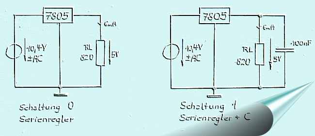
All circuits go out from the circuit in
schematic 0, a circuit, which I needed once in such a
way. The report shows, what developed from it. The input voltage
amounts to 10.4 V, which an alternating voltage is superimposed.
|
|
|
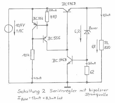
Schematic 2
is already a good voltage regulator with good suppression of
disturbances of the operating cutting. The breakdown diode of 6.2 V
forms a reference tension of 6.9 V together with the lower basis
emitter distance. The two transistors on the left half form a power
source, which supplies the basis of the serial transistor with
current.
Function:
if the output voltage rises, then the lower transistor leads more to
flow it from the power source more current rerouted into the lower
transistor instead of into the basis of the serial transistor. The
serial transistor closes increasingly. The output voltage drops
again to the desired value. And in reverse.
|
|
|
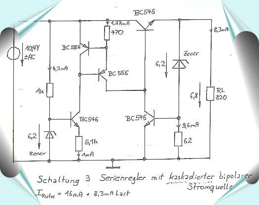
Schematic 3
developed like schematic 2. The programming of the power source of
the serial transistor takes place via an additional power source.
Thus continues to rise in particular the power Supply Rejection
Ratio still. On the load Rejection has this measure hardly an
influence.
|
|
|
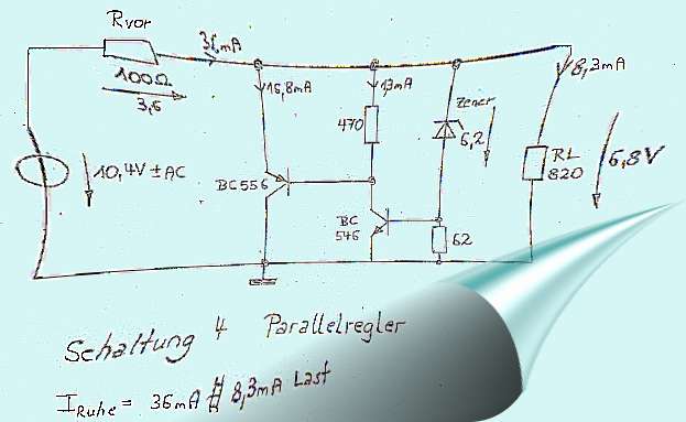
Schematic 4 is a shunt regulator. A parallel transistor
to separate the load resistance. This increased or degrades the
effective load resistance. The circuit needs a defined load
resistance. It is fast, and has the best efficiency on full load
conditions. By Rver always flows the same current.
|
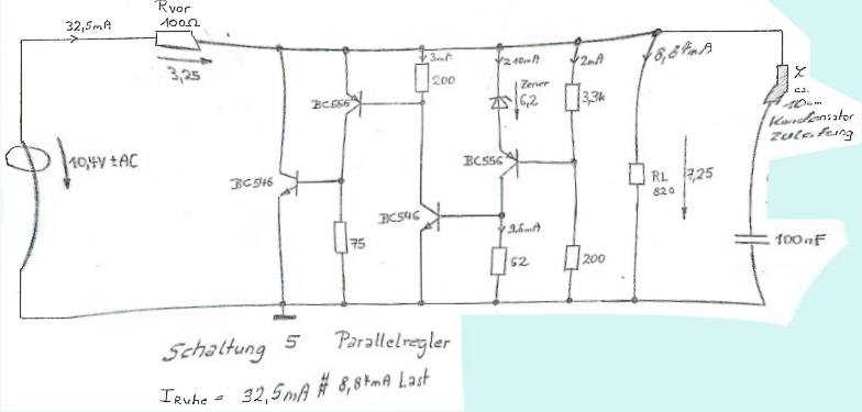
Schematic 5
is a shunt regulator with a high open loop amplifier. This circiut is
endangered for stability problems and needs a L-C combination at the
ouput. Of course there are many other possibilities to make the circiut
stable.
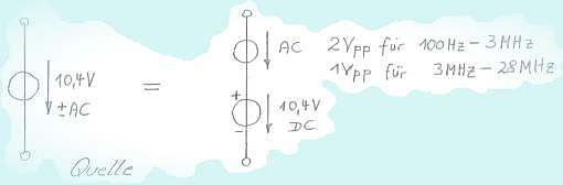
The used source, a DC voltage superimposed by a AC voltage
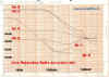
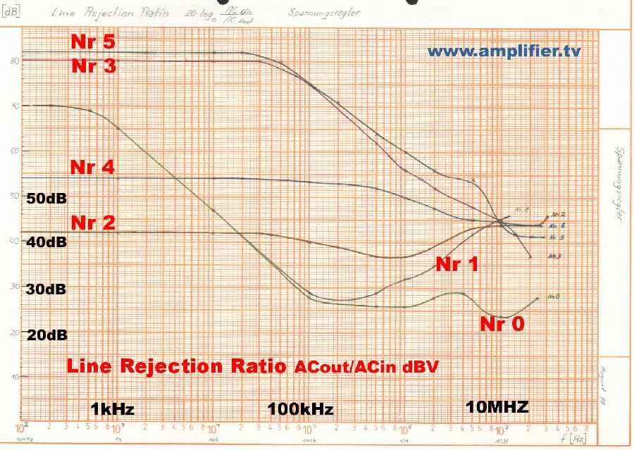
Picture shows the power Supply Rejection Ratio of
the circuits. Compared with standard voltage regulators the serious
superiority of the schematics 3 and 5 for the LINE Rejection would have
actually to be accepted by everyone without comment. Schematic 3 and 5
have high open loop into higher frequency ranges, from this exact
compensating of the disturbance results. Without question these circuits
are still easily in their efficiency optimize and improvementable.
|