
| With a -10V reference in the unipolar DAC mode the opamp covers a range of 0V to +10V. Why not testing a 0V to -10V full scale step? This requires a +10V reference. |


| Live is hard, compensations looks not fine. Switching to a negative
going output step.There is a one
division offset bias, also not readjusted. Mind starts working - what's that? Many new questions. |
|
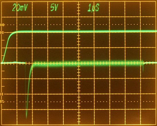
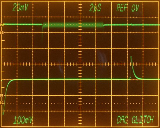
When changing the bus from 0000 to FFFF and back occurs a spike in the DAC output.
Lower Trace (100mV/DIV) shows the DAC output with two high glitches of 200mV. Upper Trace (20mV/DIV) gated settling window. A glitch has a high slew rate compared to the DAC output under normal conditions. The diode bridge rejects even this high slew rate glitch very nicely. The is not yet in in its normal operating mode. |
|
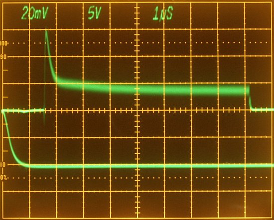
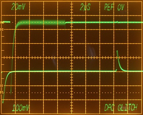
When moving the gated window to the left, the measurement system
sees the glitch like a DAC signal. The glitch is like a step function
and the DAC and op amp answer with their step response. Settling time
for this glitch seems to be approximately 2µs. |
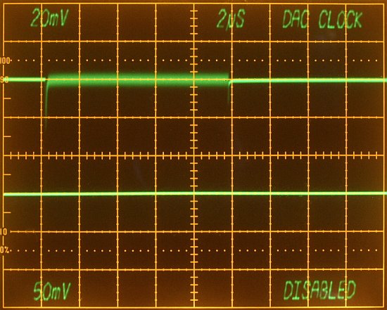
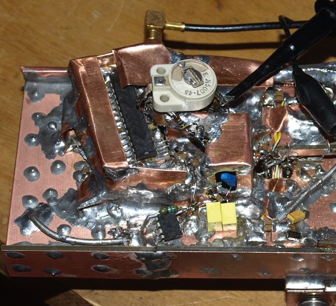
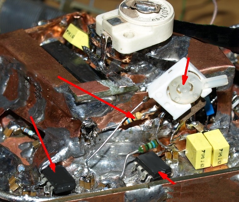
| For all these tests the DAC runs in a transparent register mode. Every code change will run through the input register and latch register directly to the output. The internal de-glitcher is disabled in the transparent mode. The transparent mode was choosen here because it's easy build up for prototyping. |