|
Important Note: My article is based on the wonderful Linear Technology Application Note AN-74, July 1998. In March 2010 another interesting LTC Application Note, AN-120 has been released. Please read both application notes for a better understanding of DAC settling time measurements. My thanks to the author and his colleagues for the excellent work. |
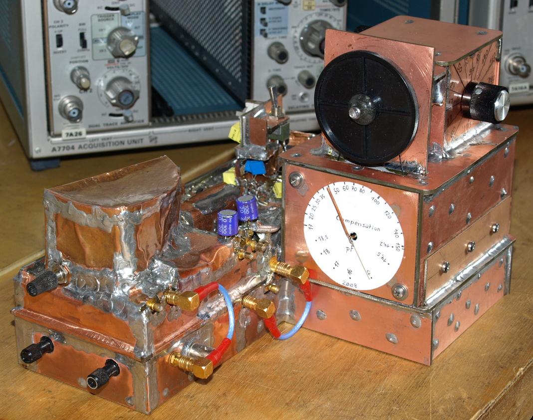
Ralf's article: - This article shows my analog hardware design technique - - My project took appr. 500 to 750 hours of private time - - Some chapters are challenging and time demanding - - 28 Chapters wit approximately 700 photos - My article wants to demonstrate my personal results align with my used hardware design technique. This is a hardware method for designing with difficult circuits, in comparison building up this circuit on a standard PCB would be a hopeless task. My article has not the intention explaining settling time measurements in detail, for this explanation read AN-74 and AN-120. Some explanations from me can be found in my older measurement article (in german or english). My article has not the intention to promote any active part. Active parts are hidden, because internet talks too much about parts in such a manner: "this part is better than this.....", I don't support this behaviour because: every part has it advantage and disadvantage depending only on the application, there is no better part or a worser part. I tried different parts, if you want to build up this AN successfully, I recommend the use of the noted parts noted in the AN-74, I used them too. My article wants to show the fun and experience you can have with analog electronic. - My shown article is a limited internet version -
|