
|
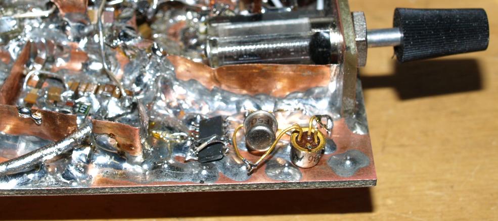
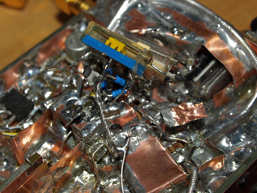
Middle - Replacing the old transistors with other types. You can't see them, they are buried under copper.
Replacing in such a way is the fastest prototyping, here a small PCB
would be of course a better solution, but this is a later step. |
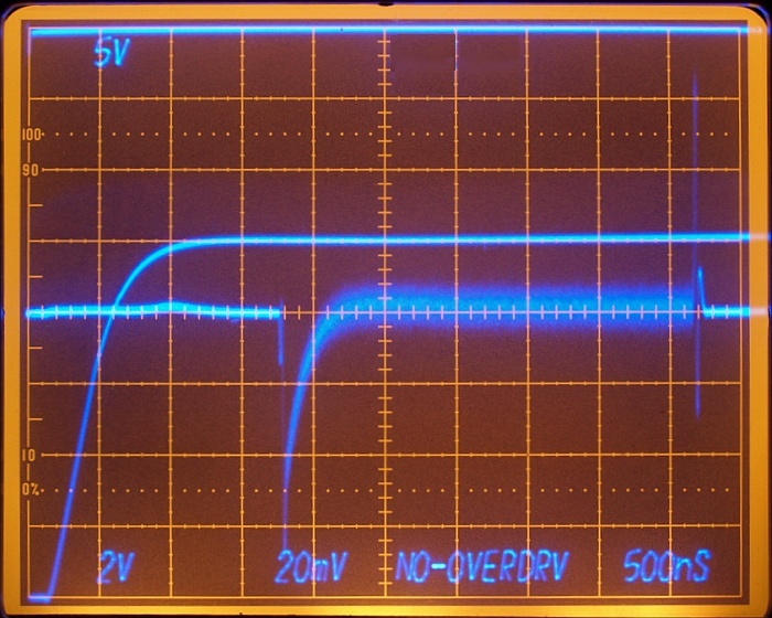
| Top Trace | 5V/DIV | Load DAC | Oscilloscope triggers on first division |
| Center Trace | 2V/DIV | DAC Output | 0V to +10V full scale step |
| Bottom Trace | 20mV/DIV | Gated Settling Time Waveform | 20mV/DIV = 500µV/DIV |
| Test Equipment - 7A26 amplifier in 20 MHz position | |||
| No Oscilloscope Overdrive | |||

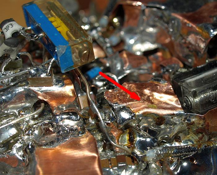
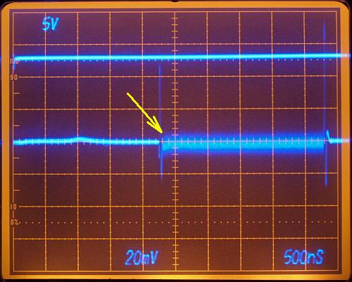
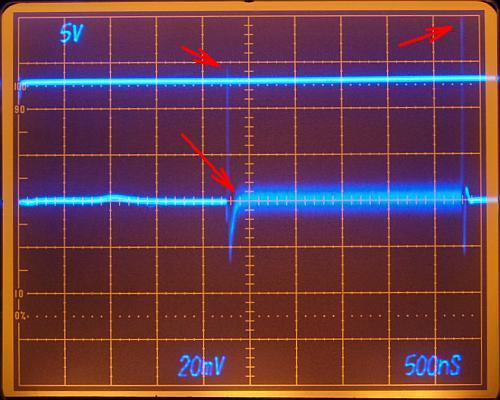
| Left photo with yellow arrow, (DAC has already settled), after swithing
ON the Sampling-Window, there is a small 200ns error on the rising
slope. Right photo (red) increased settling error and higher
transients. Such a small piece of copper on the wrong place disturbes the circuit. |
|
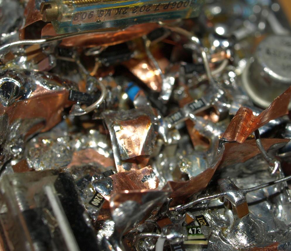
It's a funny job to solder a piece of copper on such small pads with a patch of 0.15mm. For
soldering you should glue the transistor first on the board and
then use pre-soldered very thin single copper wires and a
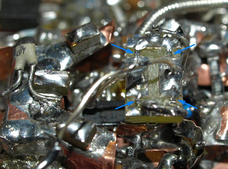
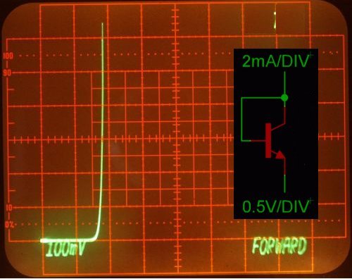
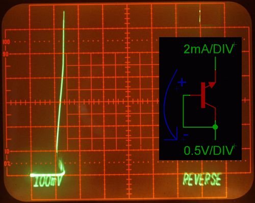
microscope magnification of approximately x20. Up to now circuit don't work, starts to oscillate and shows funny curves. I did a check on the curve tracer of these self-made diode bridge. |
|
Unfortunatel< this transitor don't work like a normal small signal
diode, in reverse connection the current breaks trough very fast. This
is the reason why this diode bridge didn't work in the circuit. |