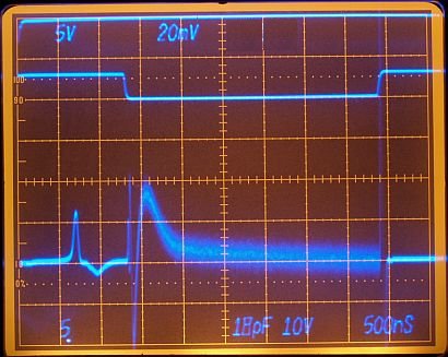
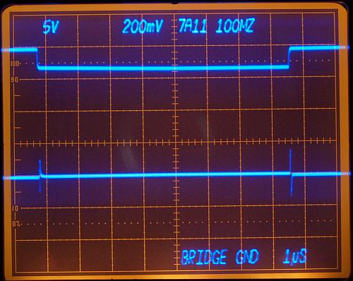
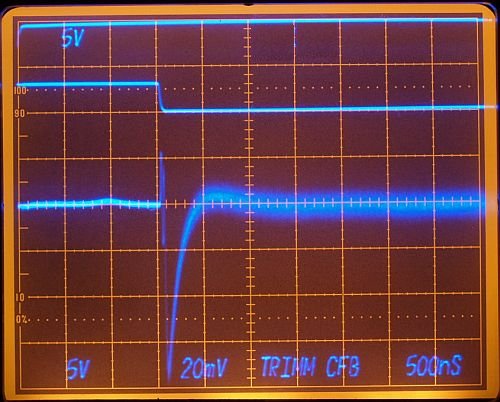
6.5 LSB/DIV 500µV/DIV Cfb=18pF 0V to 10V step
1 LSB AT Settle Node = 76µV ( 152µV AT DAC Amplifier Output )
I don't like my spikes.
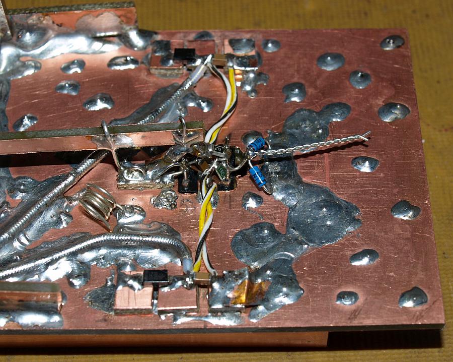


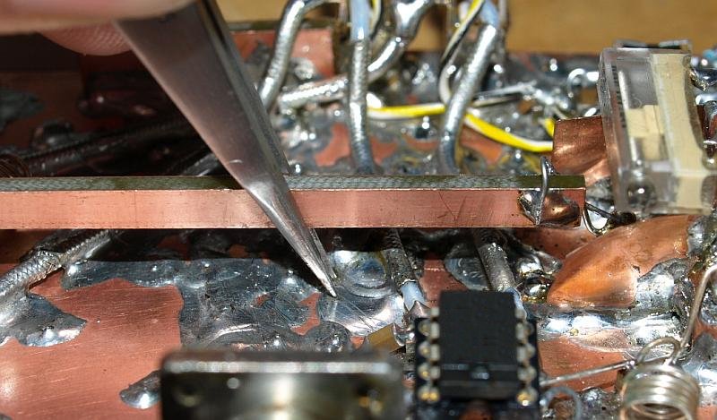
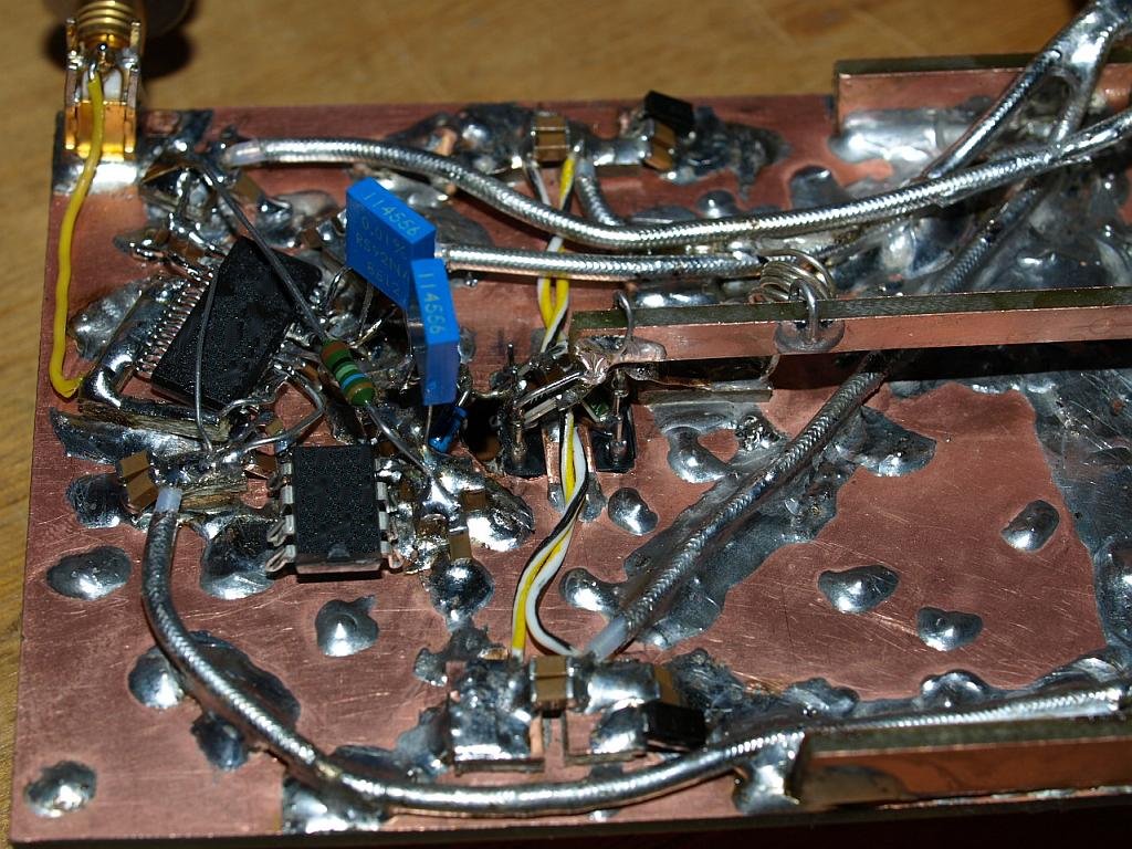
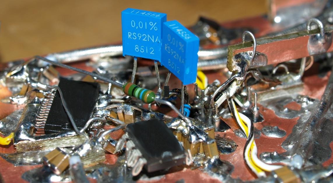
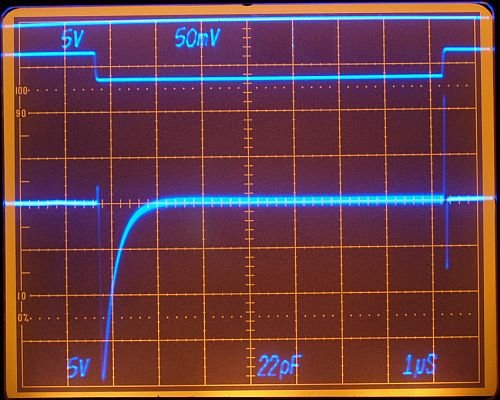
| Left - the DAC is not very easy to solder, but a SO-36 package is still solderable in such a way for fast prototyping. DAC xxxx build-up in a configuration for a 0V to 10V output full scale step. Vref must be -10V. A 16 bit DAC has a minimum resolution of 10V / 65535 = 152µV = 1LSB. |


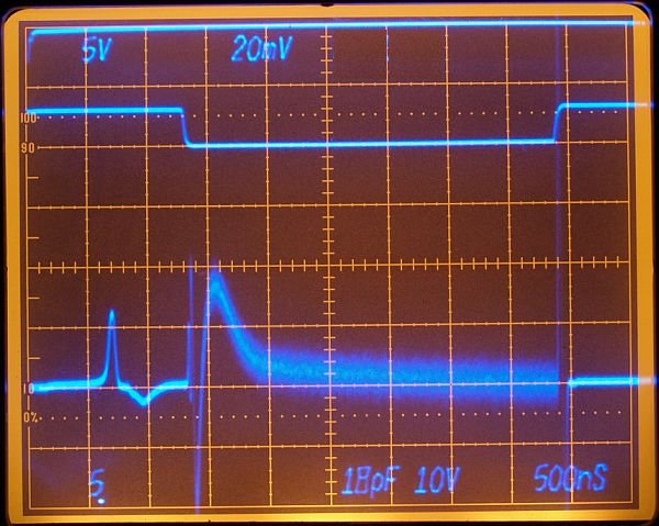
With a 18pF Compensation Capacitor the DAC amplifier seems to be overcompensated. The amplifier slews very fast, comes with a 12 LSB overshooting and settles after approximately 4.5µs. (Measurement without bridge driver/residue delay correction). (Unfortunately today the left bottom scope readout is broken - shows no "V" only a dot). |
6.5 LSB/DIV 500µV/DIV Cfb=18pF 0V to 10V step
|
|
1 LSB AT Settle Node = 76µV ( 152µV AT DAC Amplifier Output ) I don't like my spikes. |
|
|
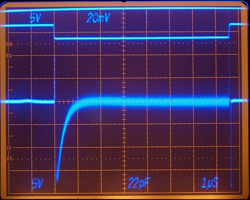
In both photos capacitor increased to 22pF, settles very nicely but
it's already overdampened. Using a 7A11 amplifier with 20 MHz
bandwidth. Oscilloscope Amplifier slightly out of range (for all
20mV/DIV measurements), a high OFF spike. |

| Settling Time about 2 to 2.5µs, oscilloscope triggered on Load DAC (Top Trace - first horizontal division). Using a 7A11 with 20 MHz. Right photo ON spike readjusted. Compensation is a demanding task, even one or two picofarad has enourmous influence. |


|
TOP TRACE - Load DAC, oscilloscope trigger SECOND TRACE - Sampling Window THIRD TRACE - DAC Output Signal FOURTH TRACE - Gated Settling Time Signal |
|
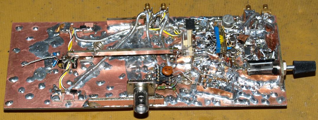
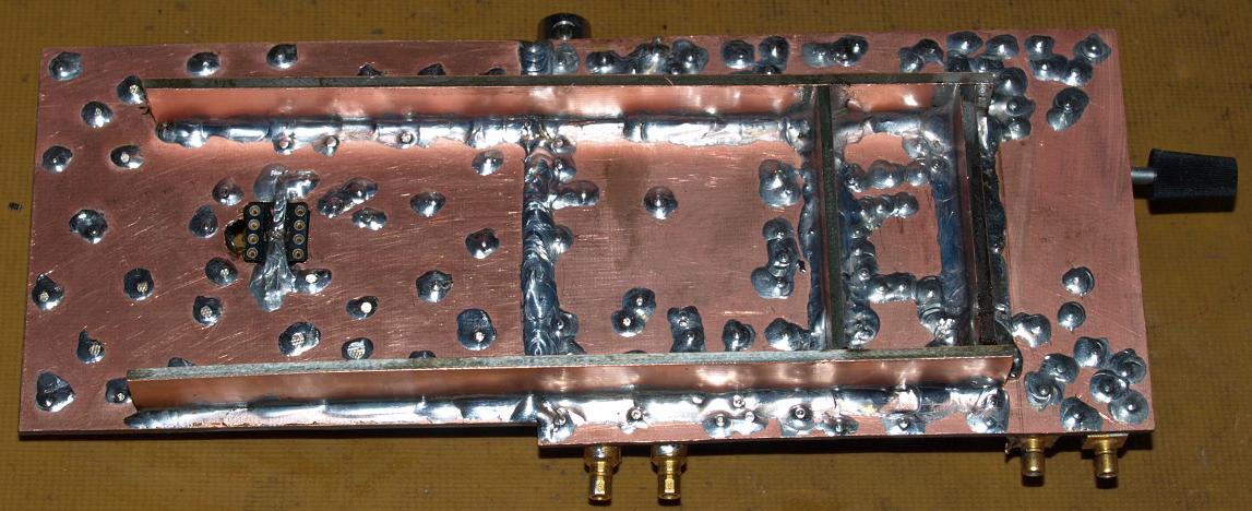
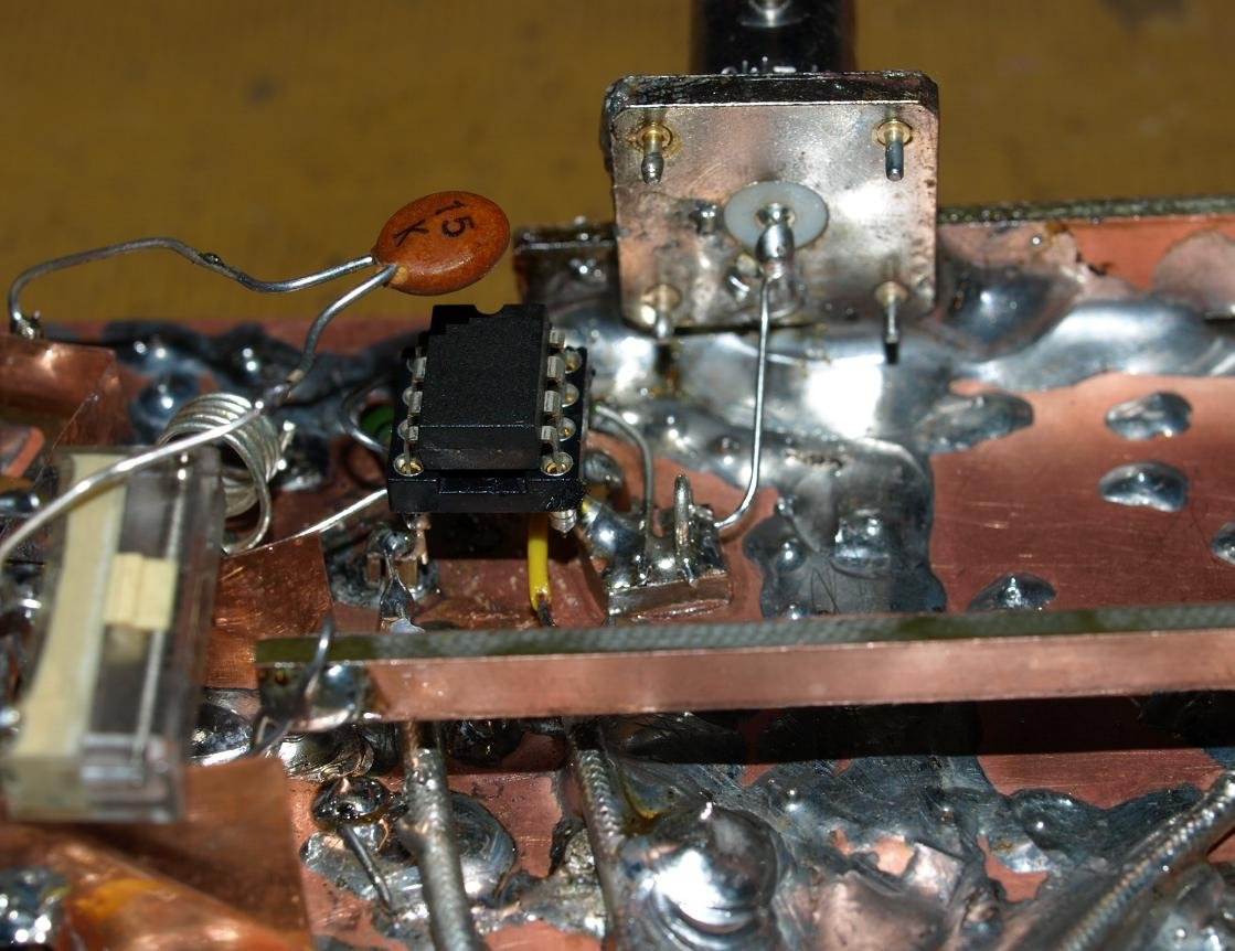
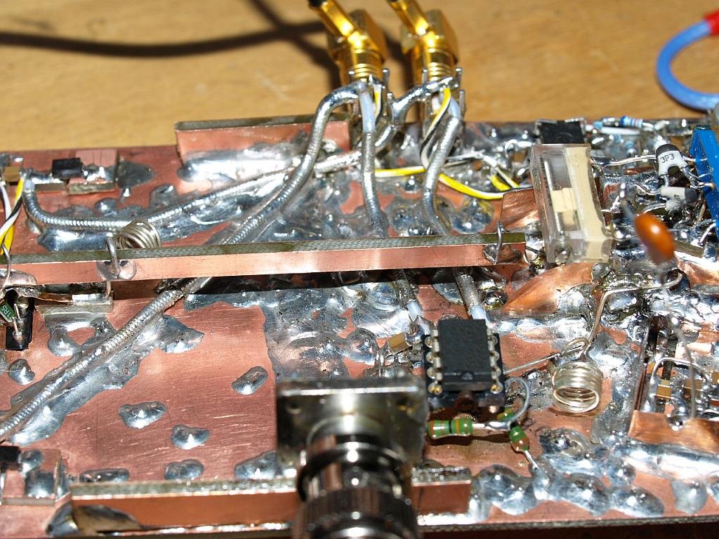
Circuit works and is useable with under basic functions. It was a hard work
building up the board and it took enough time. Experience is the gain. The spikes need to be reduced, for this I must think much about the layout and where which current is flowing - it is still possible changing the board. At the moment my ideas are empty- Another idea is the use of other transistors and diodes. |