
Differences to first simulation:
|
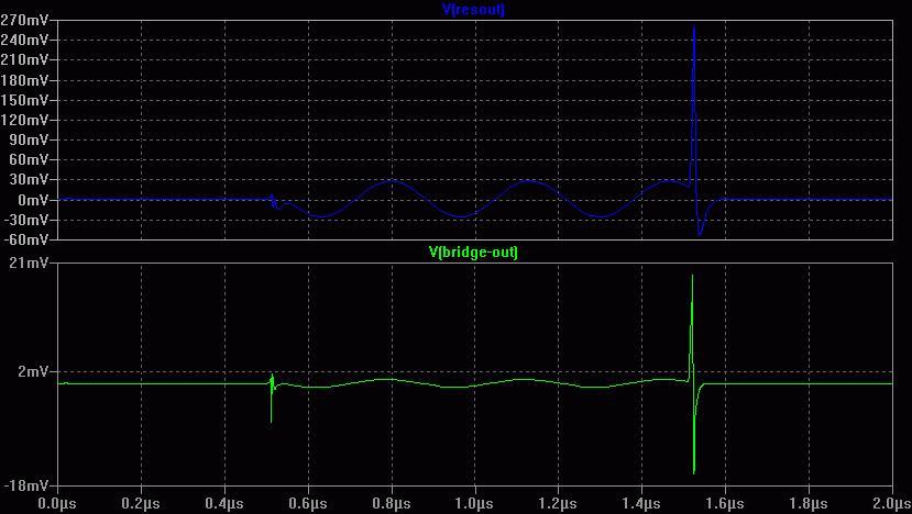
| The ON transient almost disappeared, OFF transient is still too large. AC-bal and skew setting trimmers are powerful. DC Baseline is easy to adjust. Simulation "where are transient fast currents?"I want to know if I should solder the diodes D7, D9 close to the diode-bridge-IC or close to the emitters Q1, Q2? For this I check node "ucq2" from emitter Q2. All currents flowing inside this node are positive - all currents leaving the node are negative. I(R8) less I(R19) less I(R17) less I(D6) fast transient OFF I(D3) fast transient OFF -I(D7) fast transient ON much current -Ic(Q2) high current ON, OFF ON t=0.5µs OFF t= 1.5µs |
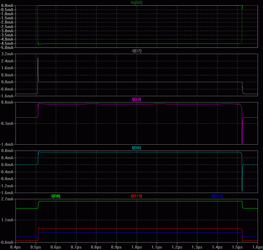
Result from simulation node ucq2:better place D7 and D9 close to emitters of Q1 and Q2 reducing influence of parasitic inductance between them. Switching diodes on is easy, switch them off is difficult - a current spike occurs, one reason: u=L*di/dtSame simulation for node ucq1:All currents flowing inside this node are positive - all currents leaving the node are negative.I(R3) less -I(R6) less -I(R7) less -I(D5) fast transient OFF -I(D4) fast transient OFF I(D9) fast transient ON much current -Ic(Q1) high current ON, OFF ON t=0.5µs OFF t= 1.5µs |
