Synchronous Step-Down DC/DC Converter

1.25A 4MHz Synchronous Step-Down DC/DC converter.

Application:

used in my FPGA core power supply 3.3 to 1.2 volt.

These circuits are really very simple to design, consider a few things and it functioned great.

Why this IC?

  • small package MSOP10 (ca.5*3mm) or DD (3*3mm)

  • high switching frequency up to 4 MHz, small inductance and capacitors. Very small ceramic capacitors with lowest ESR and ESL possible.

  • high efficiency, low heat loss

  • integrated switching transistor and diode

  • only a few external parts

  • synchronizable

  • low idle current

  • less board space

Schematic:

Schaltplan LTC3411 Abwärtsschaltregler

Figure 1 shows the schematic of the layout. Here an extended low pass filter. Already the smaller original filter configuration in the data sheet shows good results.

Layout component side:

Oberseite des zweilagigen Layout, hellrot die Masse

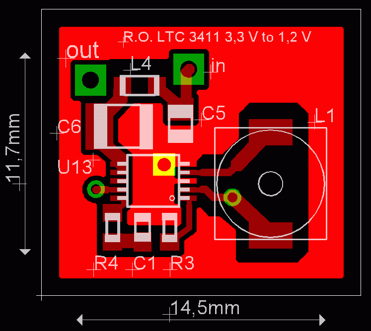
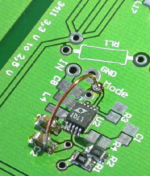
Figure 2 Layout

"Out" and "In" are soldering pads for a thin wire. Under the IC the ground terminal.

Package:

L1 shielded inductance

L4 Ferrit SMDL2012C (0805)

C1 ceramik (0603)

C5 ceramik (0805)

C6 ceramik (1210)

R3 (0603)

R4 (0603)

U13 DCDC (MSOP10)

Layout solder side:

Unterseite des zweilagigen Layout, hellblau die Masse

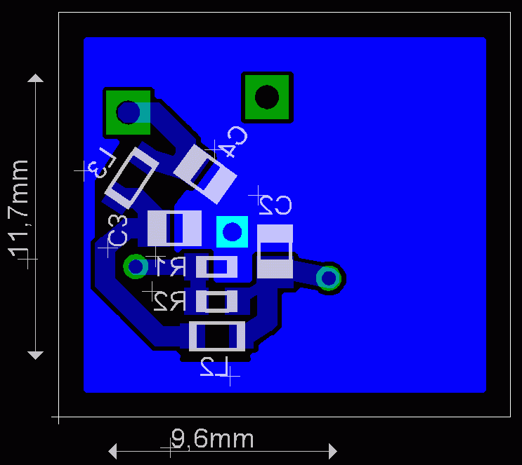
Package:

L2 ferrit SMD L2012C (0805)

L3 ferrit SMD L2012C (0805)

C2 ceramik (0805)

C3 ceramik (0805)

C4 ceramik (0805)

R1 (0603)

R2 (0603)

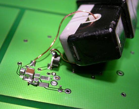
Figure 3 a simple layout

 Layout notes: make it small, the shown is a suggestion taken from my application.

Component side:

  • The ground pads is in star point connection. The connection pin 5 "Powerground" is shortest possible to the neutral point. The ground connection of the input capacitors C5 & C6 is also shortest possible to the neutral point. Important, the ground of timing parts no power currents flows in this part of the layout, no calvanic coupling.

  • The inductance L1 has distance to the circuit. Although a shielded inductance was used here, no parts should be placed on the opposite side of inductance. If it cannot be avoided, then in no case the IC or the very sensitive feedback network from R2 and R1.

  • The wires of inductance L1 should be short as possible, since in them higher frequency currents flow.

  • A parasitic parallel capacitance of inductance L1 is to be avoided.
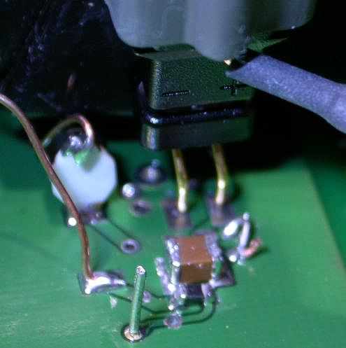
Solder side:

  • The ground connection of the output filter condensers goes directly to the neutral point, high frequency currents through these condensers hardly flows through the short piece between R1 (feedback resistance) and the neutral point.

  • R2 close to C2, long wires in the feedback network - avoid it.

  • L2 and L3 spaced layout around them to reduce the parasitic capacitance.

  • Place the low pass in the order that the resulting parasitic series inductance ESL of the capacitor is low as possible.

Fehlendes an der Schaltung:

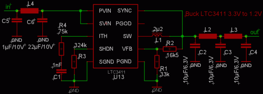
  • not used in the feedback the 22pF Lead compensation capacitor (15pF to 33pF see Figure 7 in the data sheet). Improves stability, test it. Circiut was stable without.

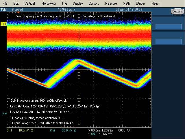
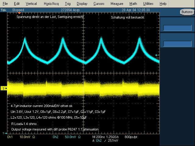
  • Pin 2 "Synch/Mode" choose operating mode: Burst - Pulse Skipping - Forced Continuous choosed here the Forced Continuous, easy filtering, works goog with a constant load. The Layout don't show the load.

Tests:

getting experience with the circuit. The photos aren't no exactly the shown layout, doesn't matter.

Versuch mit LTC3411

Lastwiderstand

Figure 4  first soldering

Figure 5  running circuit, with load resistors.

Stromzange zum Messen des Strom in der Induktivität

Stromzange und Differenztastkopf   Differenztastkopf P6247 im Einsatz

Figure 6  shows a P6042 current probe.

Figure 7 and 8  if available use an active differential probe to measure directly the real voltage vs. time on any part. Here an 1GHz P6247 differential probe. A wonderful instrument for such measurements.

Final Result  gefilterte Ausgangsspannung am LTC3411 Final Result

Figure 9  shows the final result. The output voltage under load. Scope AC-coupled 10mV/DIV. Measured with a TDS5054, using the persistance mode of the scope for half a second. Any spike within long time would be seen - but there is nothing like a spike - the output voltage is very clean.

In detail shows the sreen 467682 measurements, every 800 Nanaosekunden (80ns/DIV), totally 374ms. The rainbow colors indicating the frequency of occurrence, red is more often than blue. AC output voltage only 20mV peak peak at 1,2 Volt DC. Additional in the screen the noise of the high bandwidth differential probe. The switching frequency is hard to find, filtert out by the LC low pass.

The second sope channel displays the inductance current.

Note: don'T be confused C7, C11 and so on refer to the old test layout not the same as in the schematics here.

Tastkopf P5050 mit Masse Federklemme    Tastkopf P6139A mit Masse Federklemme 

Figure 10, 11, 12 and 13  if your are using a standard probe use a good ground. A alligator crimp is already a bad choice, it will shows you spikes, which are not there in reality. Ground your probe directly with are very short wire or a special spring.

Some other measurement results:

Spannung am Keramikkondensator

Spannung am Keramikkondensator mit optimal geerdetem Tastkopf

Spannung am Keramikkondensator gemessen mit einem Differenztastkopf P6247

Figure 14  shows the output voltage on the ceramic. Using a TDS5054 scope and a corrosponding 10:1 probe P5050. These combination has a bandwidth of 500 MHz on the probe tip. Current measured with a P6042. Measurement done with the alligator crimp for grounding the probe.

Figure 15  same as in figure 14. Only difference grounding the probe with a spring. The AC peak only 50 mV instead of 90 using the alligator crimp.

Figure 16  same measurement as in figure 14. Now using the acitve differential probe P6247. AC peak reduced to only 20mV. In figure 14 you are searching for some ghosts! never exist in reality.

Spannungsabfall an einer induktiven Leiterbahn

Wirksamkeit SMD Ferrit

Induktivität in der Sättigung

Figure 17 demonstates the voltage drop within the layout on a simple piece of wire. The differntial probe make this measurement possible.

Figure 18 shows the voltage drop on the SMD ferrite. These spikes are removed from the output voltage. What a nice part, very helpful to achieve a clean output. Useful the active differential probe, with it's low input capacitance of only <1pF.

Figure 19 shows here too much current through the inductance. The part works in the nonlinear area of the B vs. H curve. Avoid such a condition.

Have fun with your voltage regulator. Attend my words and the notes in data sheet, your regulator will work fine, it's really very easy.    deutschdeutsch

Disclaimer

www.amplifier.cd