|
A Digital to Analog Converter can be compared with a very fast
adjustable resistor divider, together with an operational amplifier the
DAC delivers depending on model typical 256 to 65536 (8 bit to 16 bit)
different output voltage steps. Settling Time is a very important parameter for every DAC and is defined as the time until the output voltage reaches and don't leaves again a defined voltage tolerance band. It is said the DAC has settled to X Bit or X ppm or X% within X time. |
|
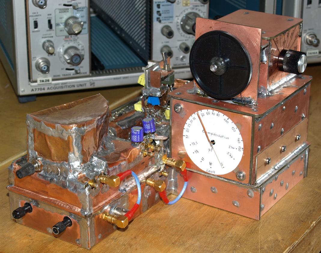
The circuit used in the shown test equipment is based on the Application Note AN74 from Linear
Technology.
In my opinion this application note 74 is one of the best
and interesting article about analoge electronic. Thanks to the
authors of that application note, I could not measure settling
time without the help of AN74. It's very recomended for the reader to download the AN74, read and get a feeling what a difficult task it is measuring settling time. The circuit got some small modifications to fulfill my personal demands, but changes are not really necessary. |
| It should be noted correct measuring the settling time is a demanding task. Especially reaching a very flat response or not to overdrive the oscilloscope takes you much time and endurance. Up to now this project took me about 500 to 750 hours of private time. The documentation shown on the website is only a small part of 350 pdf pages with a total of approximately 700 photos. Hoping this gives you a overlook about the endeavours done in my summertime 2008. It is very helpful having a perfectionistic mindset (or in other words being "a little crazy") not to capitulate from the problems experienced. |
|
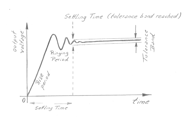
This drawing shows a possible output voltage vs. time. Load DAC signal
starts measurement at t=0 sec. The DAC output amplifier slews maximum,
as fast as possible or allowed by compensation. In the near of the
target-value the amplifier overshoots and goes back to the final value
with a undershooting, this period is called ringing. After some time
the amplifier has settled within the tolerance band. |
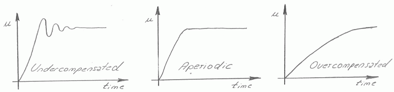
| The left drawing shows an underdamped control loop, this case has the fastest slewing and in one special setting also the lowest settling time, but overshooting must be tolerated. This system tends to oscillate on it's natural damped frequency or on it's dominating pole. The middle drawing is the aperiodic case, its exactly on the border between underdamped and overdamped, called critical damped or aperiodic case. The right drawing is already overdamped, takes a longer settling time. |
|
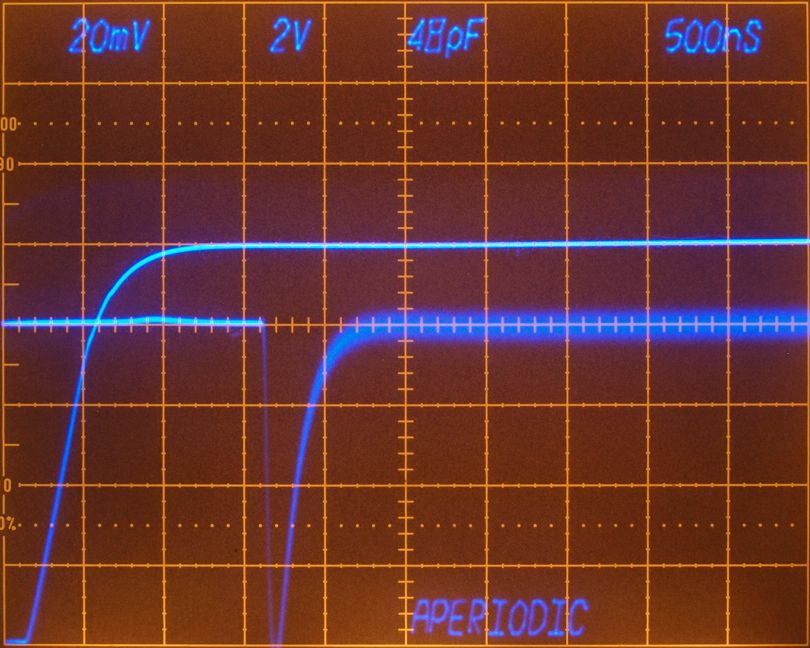
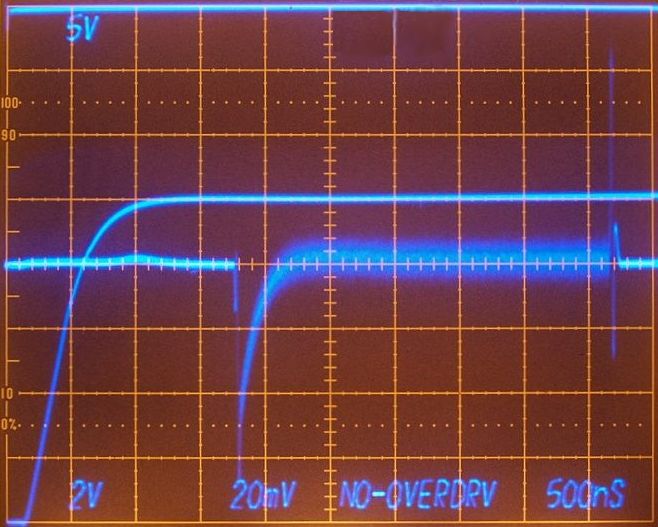
Upper Trace with 2V/DIV operational amplifier output Bottom Trace with 20mV/DIV shows a sample of the full settling period, trace shows the moment when the voltage reaches the final 16 Bit value. The 20mV/DIV signal is pre-amplified and corresponds to 1mV/DIV on the operational amplifier output. Circuit triggered on the Load DAC signal exactly at the first Division. The vertical resolution is 6 LSB/Division, with 1 LSB equal to 153µV for a 10 volt range. In this setting the amplifier has been compensated for an aperiodic setting, measured 16 Bit Settling Time 2.3µs. |
|
All shown measurements before reached their limitation due to
noise from operational amplifier, oscilloscope amplifier, DAC resistors
and the reference voltage. The non-periodic noise can be reduced by
averaging with a digital oscilloscope having this property. |
|
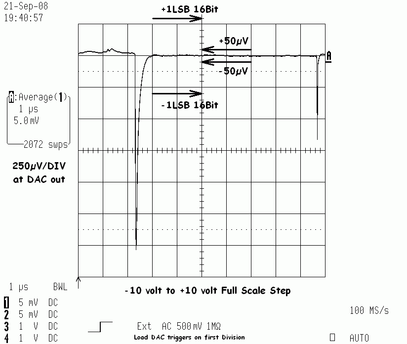
This DAC is compensated aperiodic with an ultra flat Full Scale
Response for a -10V to +10V step. The operational amplifier settles to
approxiamtely 19 to 20 Bit within only 3 Microseconds. These very
precise compensation adjustments take 30 minutes time. The oscilloscope
averaged for 2072 sweeps, this reduce the non-periodic fractions. The oscilloscope is nowhere overdriven. The negative going glitch at Division 9.6 came from switiching OFF the gated measurement window. The found compensation presents an almost ideal bandwidth limited Heaviside Step Function. |

|
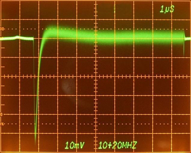
A more detailed zoom with a tolerance band of +/-10µV also for a
-10V to +10V Full Scale Step, this corrosponds to a 20 Bit (1ppm)
Settling Time within 3µs. Zoom from 5mV/DIV to 1mV/DIV done mathematically within the oscilloscope, the oscilloscope amplifier is still not yet overdriven, the trace leaves the screen range only due to the mathematical zoom. Number of averages here 2049 sweeps, an increased number of averaged sweeps can't further decrease the noise floor - the stability limit of this averaging system has already reached. |


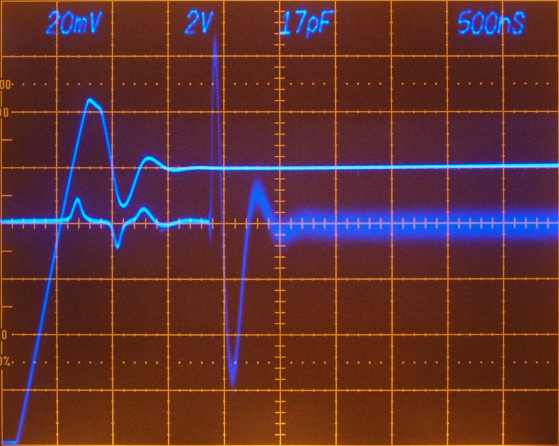
| Wrong compensation with the wrong parts and the wrong method, there are
so many possiblities that such things can happen. I was very happy at the
moment when I reached my first flat compensation, if you follow me in
my steps, you will understand the happiness. Bottom trace is the 5 volt Load DAC singal. |
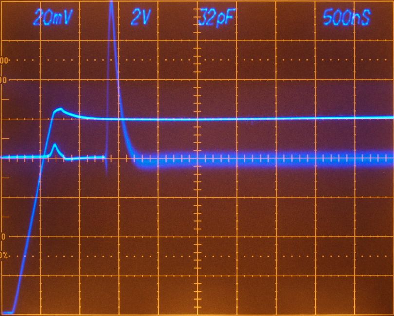
| This measurement is taken from the beginning of the project. At DIV 9.4 there is still a gated window switch OFF glitch, also at DIV 3.6 a smaller gated window ON glitch. Aber rebuilding many times the measurement channel were the glitches enormously reduded and that took me a lot of time. Recommended bandwith for a microseconds settling time is a reduced oscilloscope bandwidth of at least 10 MHz to 20 MHz. A further bandwidth reduction would slurs the settling time too much, don't do. |
|
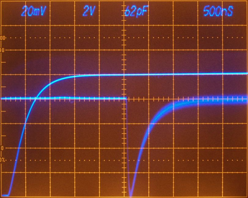
Also this compensation has still small errors, but the improvement in
reduced window glitches are already observable. This scope use a
green P31 standard phospor, the blue was a P11 phospor, Tektronix
Option 78. This failed measurements exhibited a overview about the problems which can happen during building up the equipment.
|
| If you feel like doing such measurements - don't think about it, do it - this work gives you a lot of fun and afterwards may be another level of thinking about DAC's, operational amplifers and their compensation. But never say I didn't warn you about the level of difficulties and the horrible time you will need to fulfill such a demanding measurement quality. Accept reaching this quality is very important and you should understand: target is to see the real Settling Time Behaviour of the DAC-Amplifier-Combination and not errors from the test equipment. |