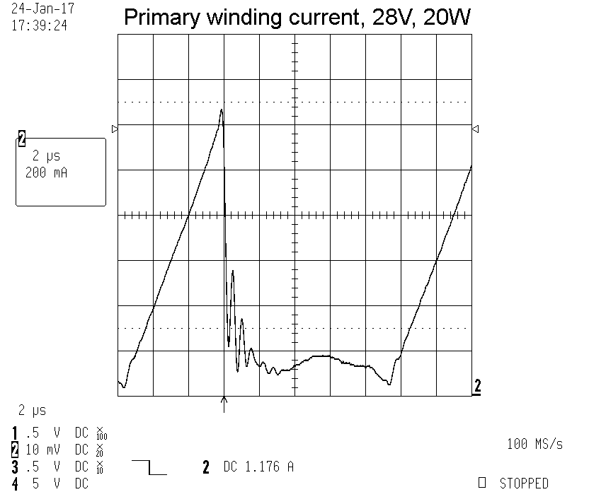
Load 16 Watt @230Vrms - Power-ON
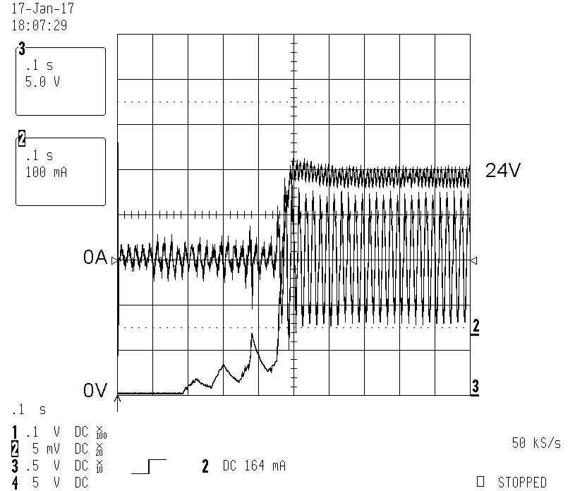
Figure 5
| Der
Bericht geht nicht auf Schaltungstechnik ein, er
zeigt am Ende auch keine nachbaufähige Schaltung, die
Bauteilenamen werden nicht genannt, unwichtig; es geht hier nur um Entwicklungsmethoden, die vielleicht
eigene Anregungen bewirken. Wer eine nachbaufähige Schaltung sucht ist auf den Seiten der IC Hersteller besser bedient und möge seine Zeit hier nicht verbrauchen. Es soll ein kleiner Überblick entstehen, was alles zu messen und zu beachten ist, bis man eine fertige Schaltung hat. Es ist eine Demoversion und daher nicht vollständig dokumentiert. In Deutsch und English gemischt geschrieben, da doch viele mitlesen möchten. Developing a Power Supply, input voltage range 90-230Vrms with 20 watt power, Power Factor Controlled. Application of this power supply is not important, board name and part names not important. This application note is not a instruction-guide or a part-guide to rebuild this circuit. Better visit IC manufactorer websites when searching for a circuit, don`t use your time to search here. The purpose of this application note is to give a short overview how many measurements are necessary to get a final circuit design. Safety Considerations: working on 400 Volt AC is very dangerous for your life, do this electronic work only when you have the skills, safety tools and when you are professional trained to work with higher voltage. Use isolating safety transformers. Don´t work allone. Warnung: Aufbau eines Schaltnetzteiles direkt aus der 230V Haus-Steckdose ist lebensgefährlich bei Berührung der Potentiale (Phase). Um diese Gefahr zu vermeiden muss die Versorgung der Schaltung aus einem regelbaren Schutztrenntransformator erfolgen. Hinzu kommt, fast alle Messgeräte und insbesondere Oszilloskope haben eine Verbindung von ihrer Mess-Masse hin zum Schutzleiter, das bedeutet sie können nicht für Messungen an der galvanisch ungetrennten Netzspannung verwendet werden, sie werden dabei zerstört, da sonst die spannungsführende 230V Phase direkt über Messgeräte-Masse an den Schutzleiter gelegt werden kann, was die Netzsicherung auslösen kann und/oder wahrscheinlich das Messgerät zerstört. Trotz Verwendung eines Schutztrenntrafos sollte man nicht vergessen, primärseitig sind Spannungen von 400V zu erwarten, diese sind bei Berührung von Hin- und Rückleiter genauso lebensgefährlich. Wer an solchen Schaltungen arbeitet muß über die notwendige Ausbildung und Werkzeugen im sicheren Umgang mit hohen Spannungen verfügen. Arbeiten Sie nicht alleine. |
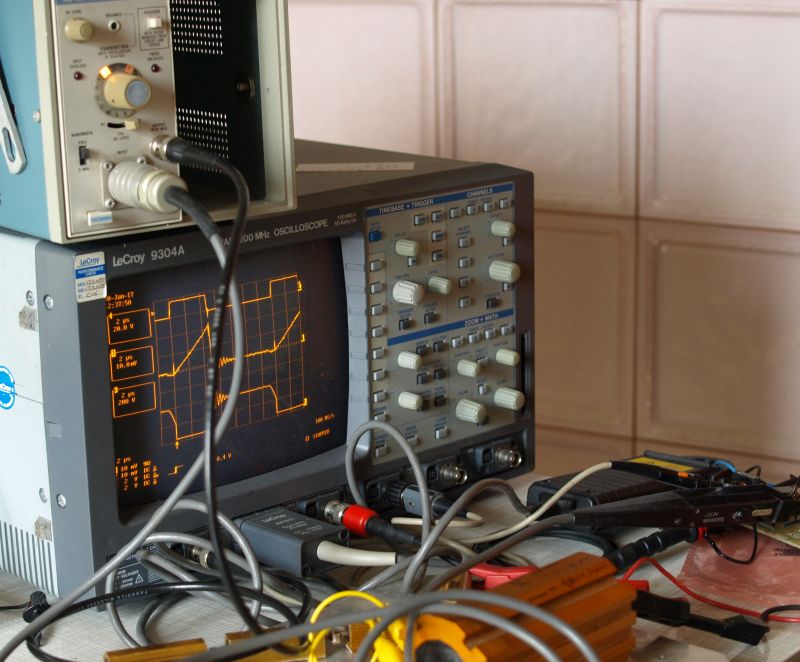
| Why
using here an older type of digital scope? When developing an unknown
evaluation board with 400V, it is a potential risk to destroy
the test equipment. Especially the first hours when getting experience
with the board are the worst. One known problem, accidential misuse
measuring on the wrong potentials on different grounds. Using safety
transformers is an additional must. Oscilloscope here has a max. 250Vpk input voltage range, 1:10 and 1:100 probes can extend the range. For me a risk using more expensive higher bandwidth models having only 100Vpk. input voltage range - avoiding tears of pain after an accidential misuse. This older type, year 1997 has enough performance for such a development, easy to operate and trustful measurement results, it is still an excellent oscilloscope. Warum verwende ich hier ein Digitalspeicheroszilloskop das 1997 gebaut worden ist obwohl moderneres zur Verfügung steht? Weil es für diese Aufgabe technisch ausreichend ist und mehr kann als nötig. Der Hauptgrund sind die vorkommenden 400 Volt am Evaluation Board. Trotz Verwendung von Schutztrenn-Transformatoren und geeigneten Tastköpfen sind beim Messen schnell Fehler passiert und manche moderne Digitalspeicher Oszilloskope wären am Eingang leicht zerstörbar. Dieses Modell hier hat wenigstens 250Vpk als Maximum, mit 1:10 und 1:100 Tastkopf noch höher. Warum soll man sich ein teueres moderneres Modell mit mehreren GHz Bandbreite riskieren, dass nur 100Vpk als Maximum aufweist? Ja, es würde mehr Spaß damit machen, aber das Risiko ist mir zu hoch - außerdem ist das gezeigte Oscilloscope leicht bedienbar und liefert absolut zuverlässige Messdaten. Noch ältere analoge Oszilloskope haben oft noch höhere maximal zulässige Eingangsspannungen, wäre natürlich klasse sie zu verwenden, nur ein wenig dämlich in der Verwendung bei single shot Signalen, wie sie hier bei einer PSU häufig zu messen sind. Momentan kann ich nicht auf einer großen Werkbank entwickeln und entsprechend ausbreiten, geht zur Zeit nur auf kleinstem Tisch, da ist der Platz zu haushalten. |
|
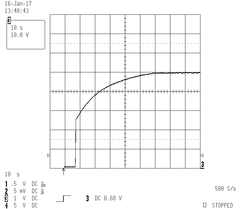
Power
ON without load, voltage should be 24V.
Increase slowly to 50V ! without load, danger by overvoltage.
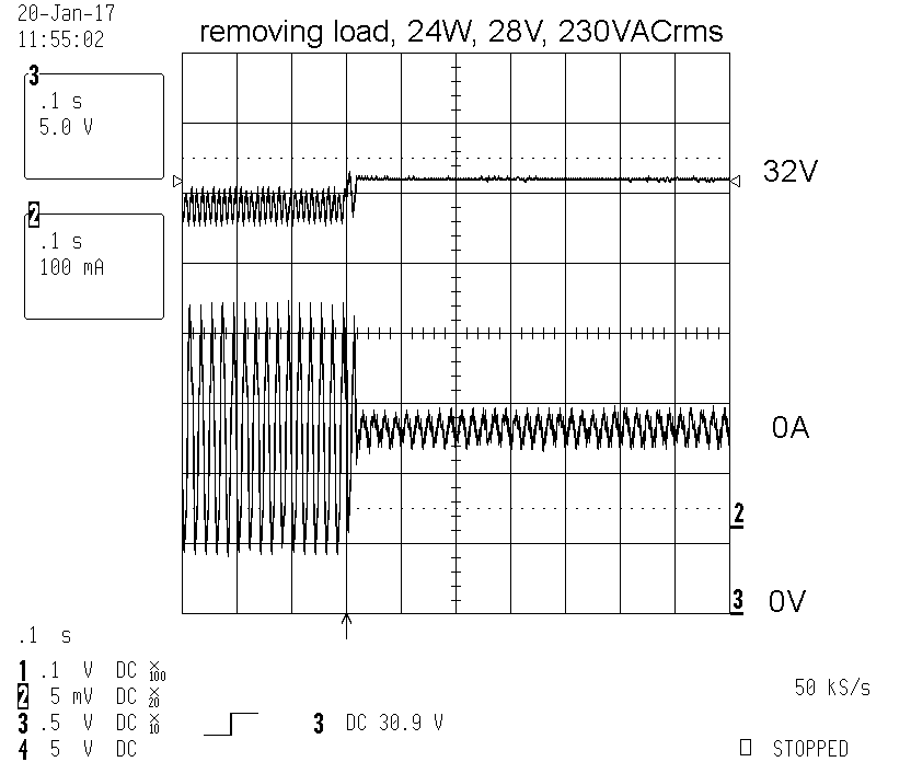
Beim Einschalten ohne Belastung am Ausgang läuft die Spannung ganz kurz auf die Sollspannung von 24V, um danach langsam auf 50V anzusteigen. Bei leichter Last kann man sich dadurch ganz schnell die angeschlossene Last zerstören. |
|
Ch2 = output voltage
Ch1 = primary current 3k6 ohm load Starts fine. Power Factor Controller reduce inrush currents.
|
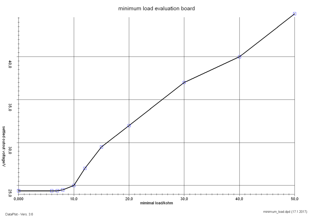
| Doing
an experiment,
starting the power supply with different minimum output load
resistors. Evaluation Board needs at least a minimum load of 8
kohm. Min. Output Power (24V)²/8k2 = 70mW. |
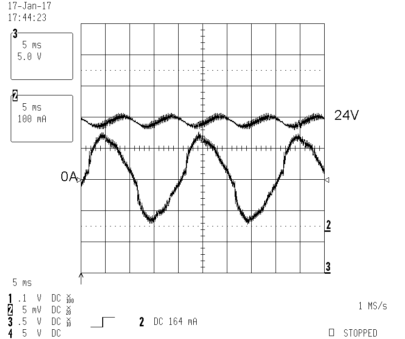
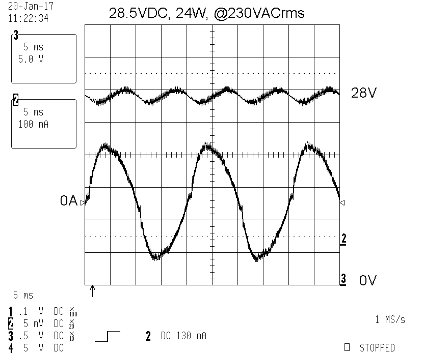
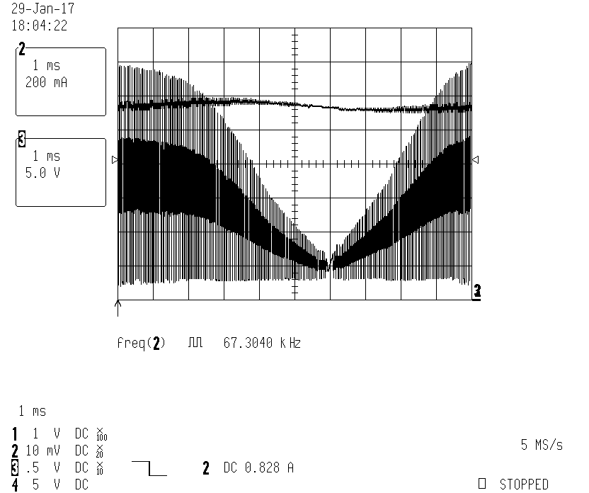
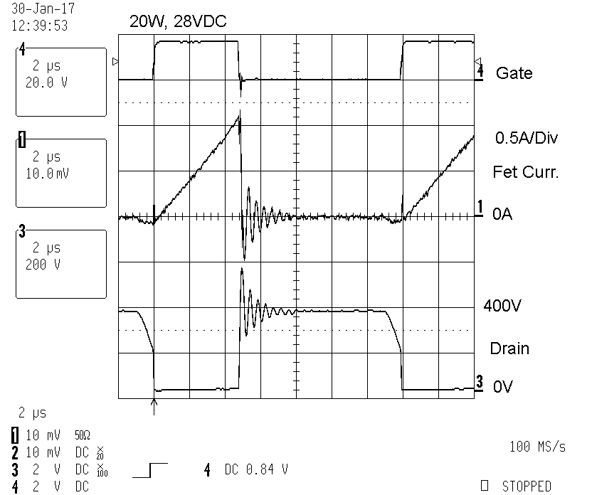
| Load 16 Watt, 24VDC @ 230VACrms Channel 2 = Input Current Channel 3 = Output Voltage User decides if output ripple +/-2V acceptable, depending on application. |
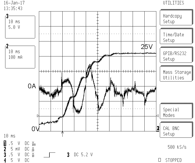
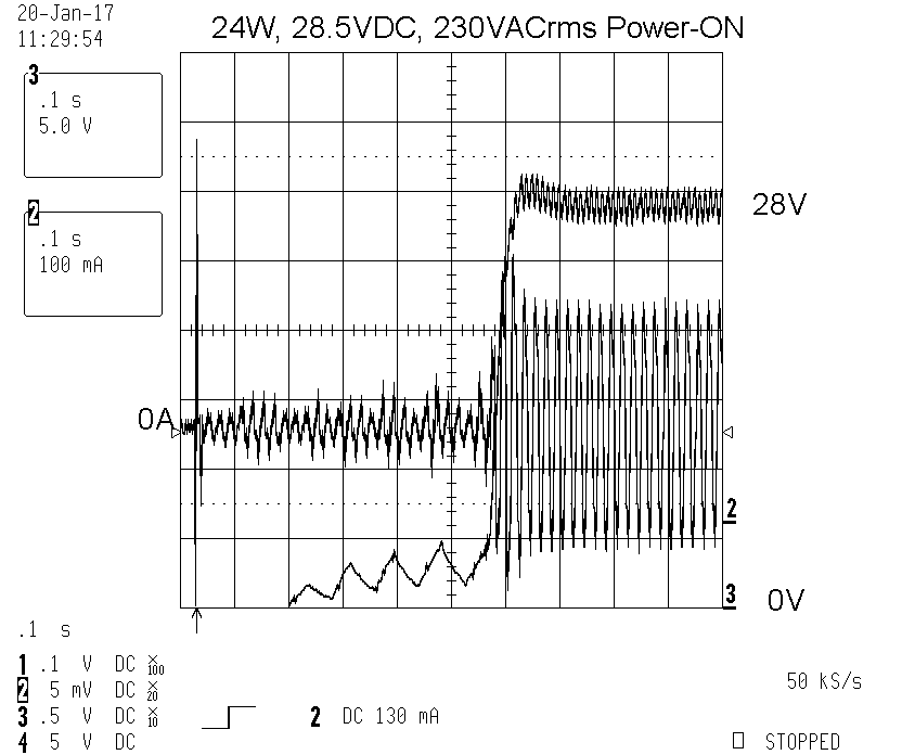
| Fine Power-ON procedure Channel 2 = Input Current Channel 3 = Output Voltage Current peak at t=0 comes
from small filter foil capacitors in the primary EMC filter. During
start-up input current remains low. Output voltage settle to a
stable value, overshooting to 26V.
|
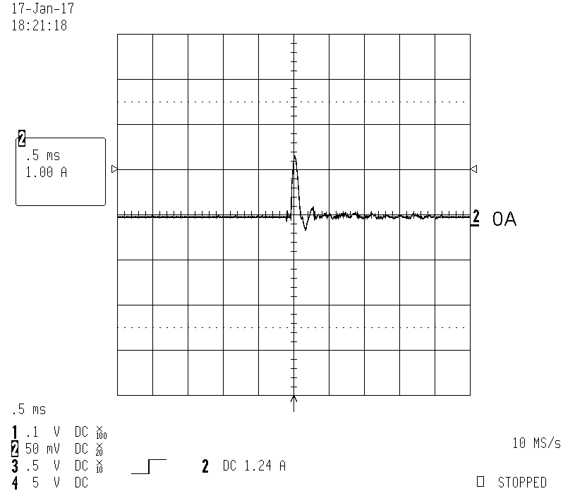
| Channel 2 = Input Current of EMC foil capacitor First
current peak at t=0 comes from filter foil capacitors in the
primary EMC filter. Input current should be considered when driven by
small semiconductors, should always remain within the drivers safe
operating area.
Peak current depends on phase angle of the input sine wave. Catching a trigger at >1A, ten times Power-ON applied. Finding the maximum possible peak current requires a equipment, switching ON under defined phase angle. |
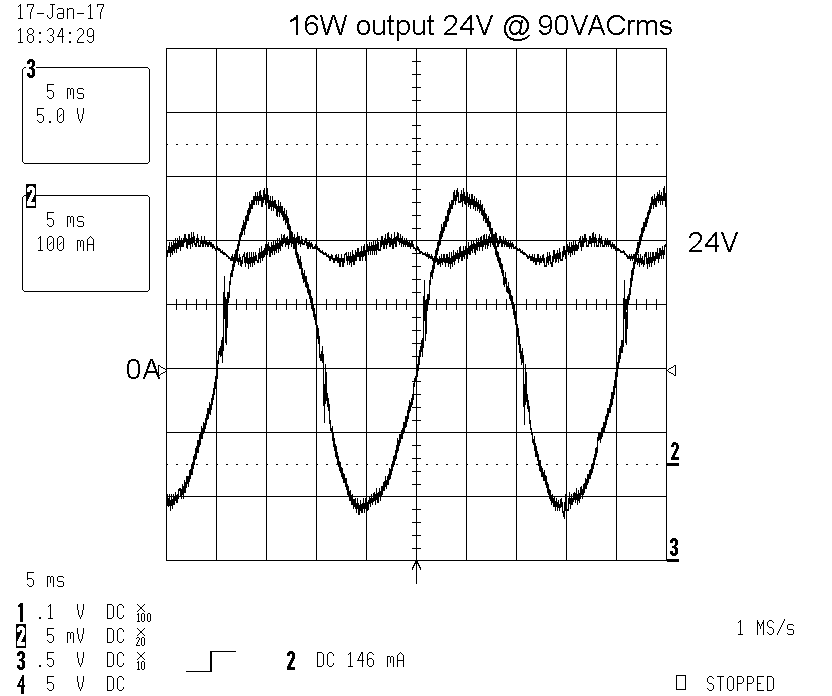
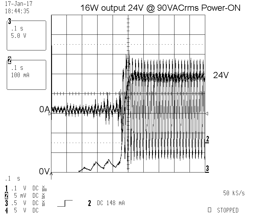
| Load 16 Watt, 24VDC @ input 90VACrms Channel 2 = Input Current Channel 3 = Output Voltage User decides if output ripple
+/-2V acceptable, depending on application. Output looks exactly the
same as with 230VACrms. No remarkable heat in any component.
|
| Fine Power-ON procedure Channel 2 = Input Current Channel 3 = Output Voltage During start-up input current remains low and
settle to the nominal level after start.
Output voltage settle to a stable value, overshooting to 26V.
|
Das Board läuft schön. Man sollte anfangs immer erst alles grob durchtesten, bevor man an die Details geht. Es geht auch darum, auch Schwachstellen kennenzulernen. |
| Power Transformer and
secondary side rectifier diode runs too HOT under 24W constant load,
these parts can not be used for a permanent 24W load, possible for a
short-time. What is short time? Can not answer this question, depends on environmental temperature, thermal mass of transformer and diode heat sink - not a question of today. |
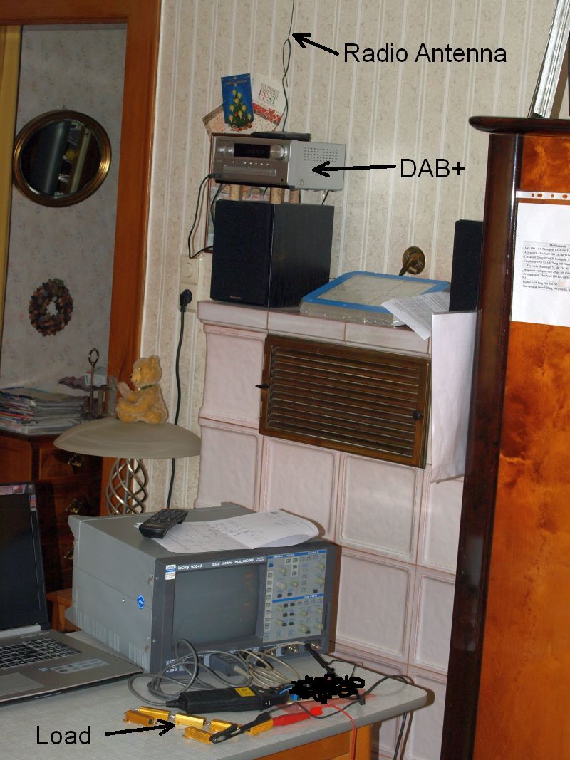
| When running the
Evaluation with 24W load there is an EMC problem. The radio on the
photo is a digital radio with DAB+ standard. One station
"xxx" stops receiving when the Evalboard is loaded with overpowered 24W. Transformer has been exchanged, additional using too long transformer wires, can be a reason. When increasing the distance between radio and Evaluation Board (antenna up, like in the photo), the radio program received clearly. Before the antenna was hanging down, this was too near. |
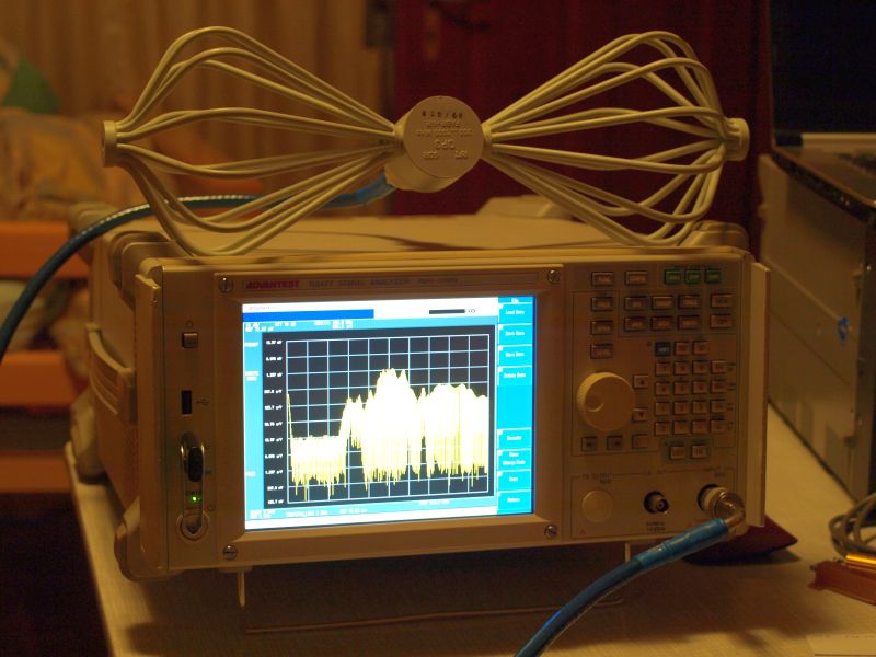
Signal Analyzer
|
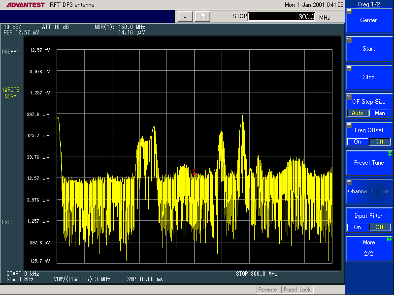
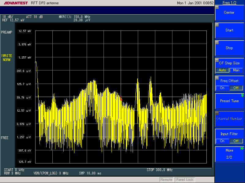
| Environmental
spectrum with antenna, Evaluation board switched OFF. Left side
9kHz, right side 300MHz, 30MHz/Division, sweeptime 10ms. 87-108 MHz, UKW radio
170-220 MHz, DAB+ radio |
|
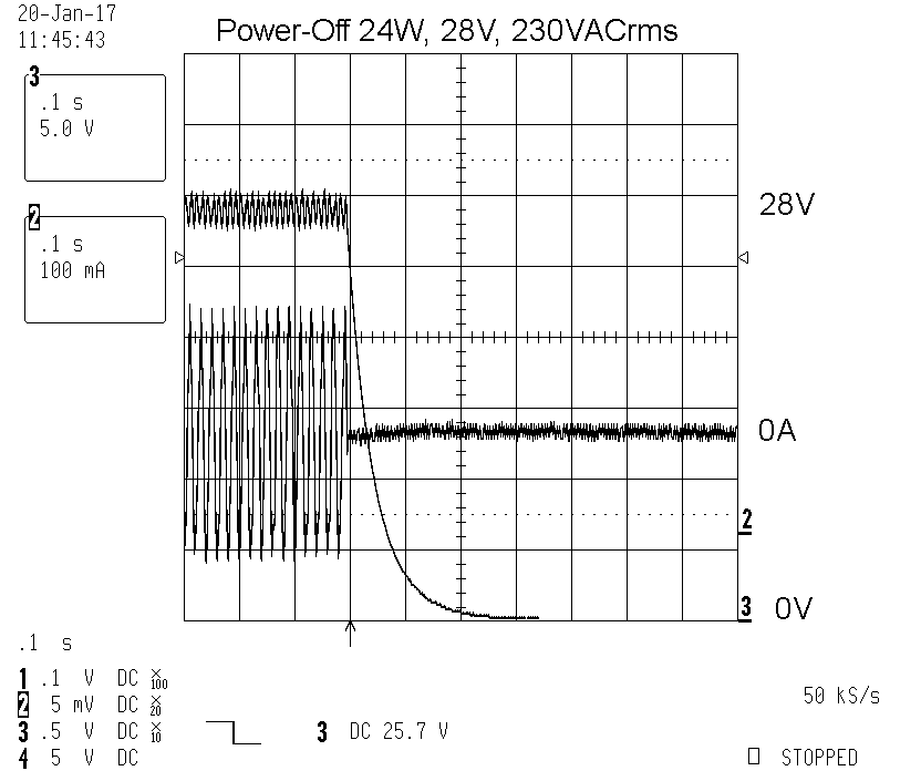
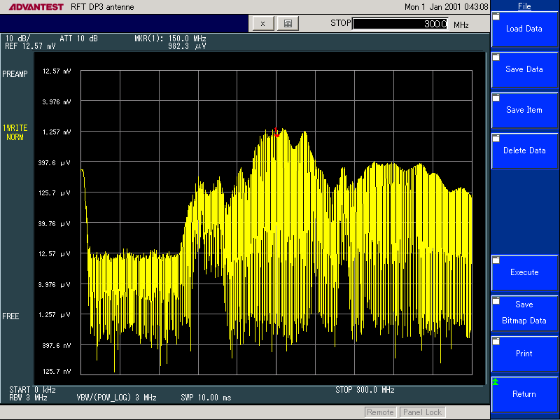
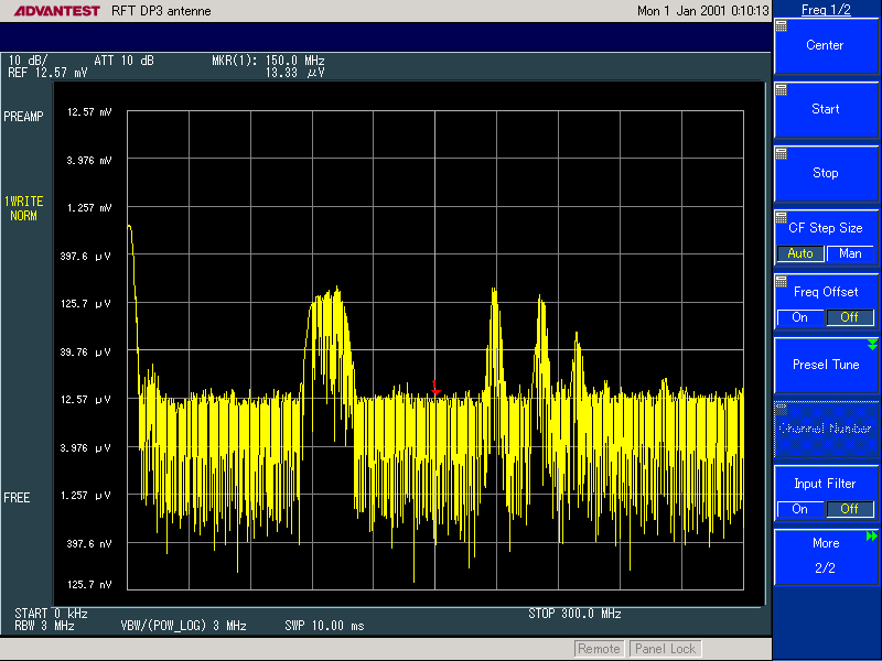
Evaloard powered-ON (24W, 28VDC, 150VAC rms)
Antenna position and analyzer setting same as figure 15. Antenna distance 1 meter to Evalboard
100-300 MHz disturbed under a short distance. When moving the antenna away, EMC level decrease rapidly. Above 300 MHz less radiation (not shown here), no harmonics in the mobil phone frequency range observed. Performance of the Evalboard:
"good power efficiency + single layer layout + unshielded parts = fine BOM, difficult EMC"
Always a demanding development task:
BOM, space, heat-management, different loads, EMC. When
developing a circuit with fast changing currents und voltages always
use a spectrum analyzer to observe the circuit, beginning
from the first hour of the development.
|
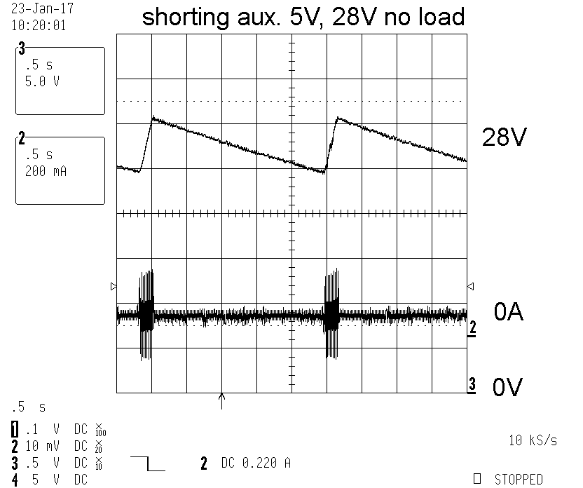
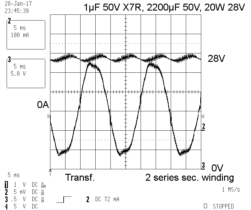
| Board has a 28V/24W power winding and 5V/4W auxiliary winding. In Figure 17 there is no load on the power winding and a short in the 4W aux. winding. Question, does the controller detect the short cut? Yes, controller detects a short-cut via the second primary winding and shut off. Results in an ON-OFF oscillation. Transformer windung runs not hot, no other part runs hot. Controller has a fine short-cut behaviour. |
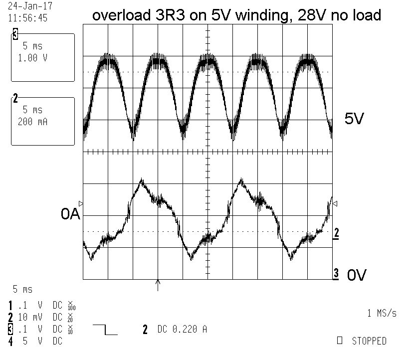
| 5V aux. winding with a
constant applied 3R3 (7.5W) winding overload condition. Controller can not detect this 7.5W overloaded auxiliary winding (overcurrent detection starts at 24W). Result:
Application requires another
type of transformer with a single secondary winding only. 5V auxiliary
voltage must generated by a DCDC converter with internal overload
protection, converter driven by 24V.
|
| Simple EMC test of a worldwide input 120W power-supply from a flatscreen television, made year 2014. |
| Air spectrum with powered-OFF TV power supply, line cable removed from wall socket. Visible the local FM stations and DAB+ stations. Span 9kHz-300MHz, sweeptime 10ms. |
| Powered-ON TV power supply. Span 9kHz-300MHz, sweeptime 10ms. |
|
Primary winding current
Off-resonant controller, fast current change. During MOSFET Off current stops fast, resulting in LC-oscillation of primary winding leakage inductivity with MOSFET capacitance. MOSFET Drain-Source
capacitance + 220pF SMD capacitor. LC resonant period 500ns.
MOSFET switching period 15µs (90VAC rms), decrease to 12µs (230VAC rms). |
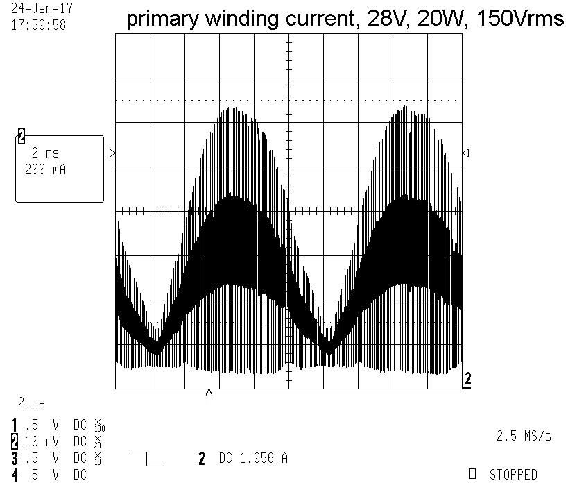
| Primary winding current follows the sinewave envelope. |
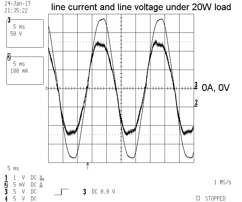
| Line current and
line voltage under full load. Power Controller ensures that the load
behaviours like an ohmic resistor, line current and line voltage
should follow each other in phase, the waveform should look the same. |
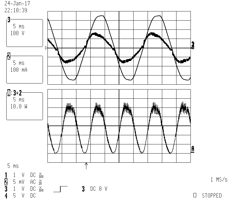
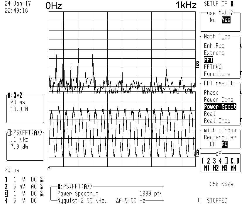
Line
current and line voltage multiplied to power. With an ideal PFC
controller and ideal sinewave voltage the power signal should be a 100 Hz
x²signal. Power Factor is distorted in the maximum power
area.
|
| Power Transistor
changed with another SMD 800V/1A MOSFET (cheapest price). A small piece of
copper-foil acts here as heatsink. Copper becomes very warm under 20W
load and low input voltages, my finger burns when touching, too
hot! For a final PCB version this small SMD transistor would require a PCB-layout heatsink area large as possible. Enough thermal vias to the inner-layers highly recommended. The heat sink is connected to the Drain potential. Drain-to-Source Capacitance reacts with the parasitic transformer incductance as LC oscillator used in this ZCS Zero-Current-Switching system. In the first "valley" switch the transistor. |
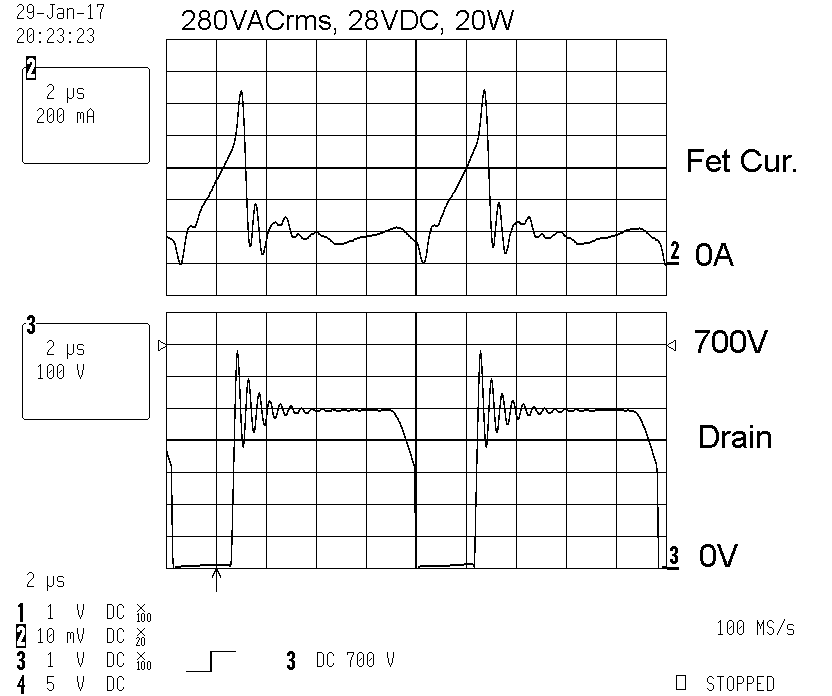
| Fly-Back,
results in high Drain-Source voltages. When driving the
Evalboard with 280VAC rms the Drain voltage increase up to 700V. MOSFET transistor has a 800V specification. 700V is large and a dangerous number. When doing the layout this high voltage has to be considered in surface-leakage and isolating distance. Also when measuring such a high voltage use a 100:1 probe, the used probe has a 1,5kV specifiaction. Don`t use 10:1 probes, many of them are not specified for 700V, can damage oscilloscope input.
|
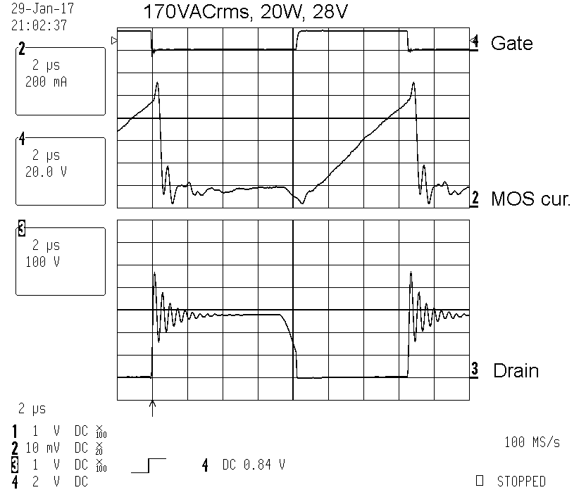
| Before in Figure
30 the drain current is not correct measured, the bandwidth of the
power current probe (max. 150A, 120kHz) is too low. Therefore for the
fast changing drain current a 50MHz type. |
| Fast drain current changes measured with 50MHz probe. Drain current (Ch.1) and Drain voltage (Ch.3) are now exactly in phase. step 1.----------------------Gate ON------------------------------------- When switching ON the Gate, current in the transformer starts with a ramp. Current increase linear, a good message, the inductance of the transformer remains constant even under higher currents, core is not overloaded. An overloaded core would show an non-linear ramp with a fast slewing ramp under high currents. step 2.---------------------Gate OFF------------------------------------- After reaching a maximum current level (detected by the controller) the Gate switch OFF and stops continuing charging the core with magnetic energy. Current in the winding stops very fast, Gate goes low with fastest slew-rate possible by the controller. For the gate discharge there is no smd resistor in the gate, only a small signal diode, fast OFF.
For the gate charge there is a 220ohm resistor in the gate, resulting in an slower ON. Gate OFF must be done as fast as possible to keep the MOSFET switching loss to a moderate level. Consider when switching OFF the MOSFET the Drain voltage is low, but the Drain current is at a maximum. OFF switching-power = draincurrent*drainvoltage
Disadvantage for the fast OFF switching, increased EMC emission: Drain current changes very fast, large high H-field emission. Drain voltage changes very fast, large E-field emission. step 3.---------------------Oscillation----------------------------------- Transformer leakage inductance and MOSFET drain capacitance starts LC resonance step 4.---------------------Demagnization------------------------------- stored magnetic energy in the transformer core runs empty (energy transfer to secondary side). When energy transfer stops (stored magnetic energy empty), voltage at the primary winding increase with u=L*di/dt. An increasing reversed voltage across the primary winding reduces automatically the drain voltage. This automatically decreased drain voltage can be observed as the slowly falling drain voltage ramp. The controller does the same, measure and search for a moderate -du/dt drain voltage. After detecting this demagnization point the controller will ON the MOSFET again. step 5. ------------------------ON-------------------------------------- exactly after core demagnizited (empty magnetic energy) it is a nice moment to power ON the core again. At this moment no current is flowing in the primary winding and no drain voltage (voltage across coil), it is an ideal point, less MOSFET switching losses. Because drain voltage and current is low, the gate can be switched ON slowly, thats why there is a Gate-ON 220 Ohm resistor, reducing the MOSFET ON time. Swichting ON creates not much MOSFET switching losses and not much EMC-emissions, this is an advantage. MOSFET Power OFF creates much EMC-emission and much thermal Switching-losses. MOSFET Power ON creates less EMC-emission and less thermal Switching-losses. ZCS (Zero Current Switching) method: approx. 50% of the EMC-emission and thermal Switching-loss could be reduced under MOSFET ON. Remaining 50% EMC-emission and thermal Switching-loss during MOSFET OFF can not be reduced. E-field and H-field emission can be only reduced, using a larger slower switching MOSFET with a larger thermal heatsink and less power efficiency. It is a question of the application what is more important: less EMC-emission or a better power efficiency. |
 .
.