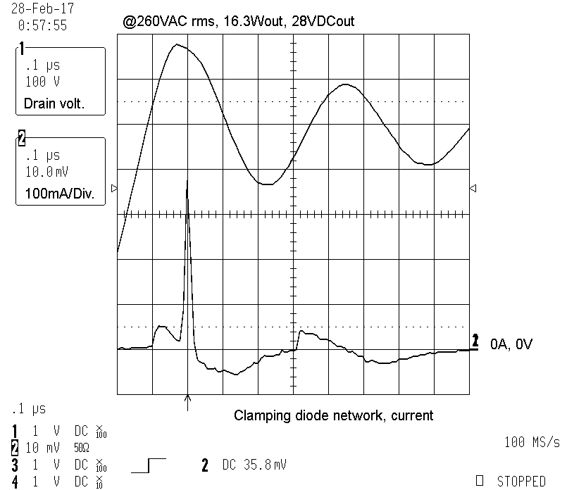
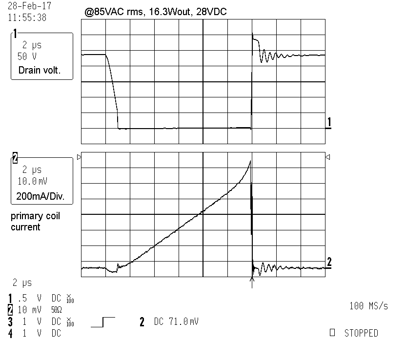
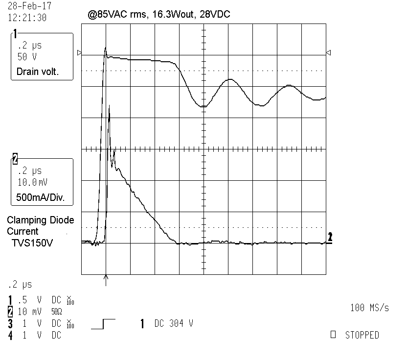
| Current in clamping diode network. Two TVS diodes (150V+150V) connected in series. 1.7Apk under high line voltage |
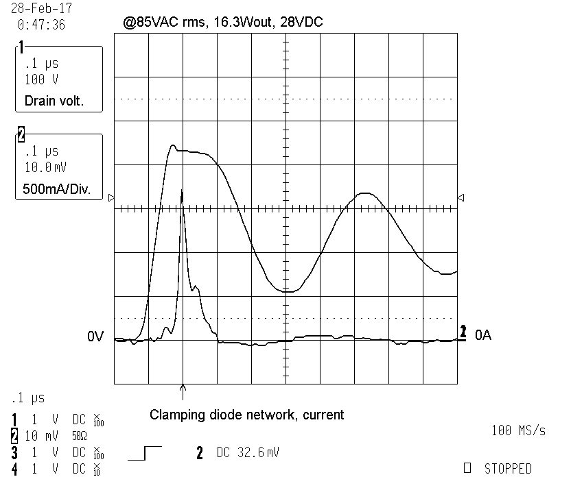
| Board
came in a slight modificated condition. The diode clamping network made
of 150V + 150V TVS in series. 400mApk under low line voltage |
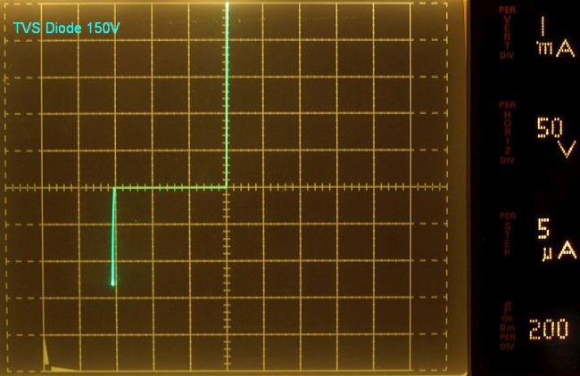
| I vs. U curve of a 150V TVS diode on a curve tracer. |
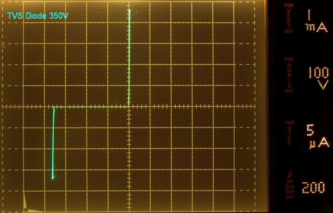
| 350V TVS Diode I vs. U curve |
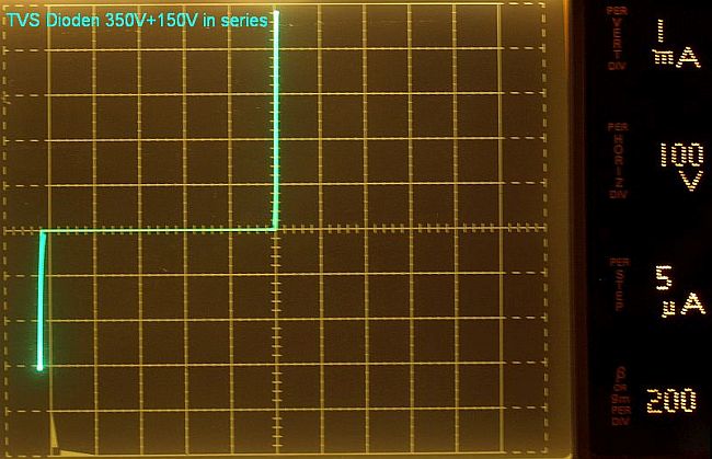
| 350V+150V TVS Diode in series connection I vs. U curve |
| Using now only one 150V TVS Clamping Diode. |
| With
only one clamping diode (TVS150) hard clamping. Drain voltage reduced
compared to 150V+150V solution. More current in the clamping diode. |
| With only one clamping diode (TVS150) more clamping action. Drain voltage reduced compared to 150v+150V solution. More current in the clamping diode. |
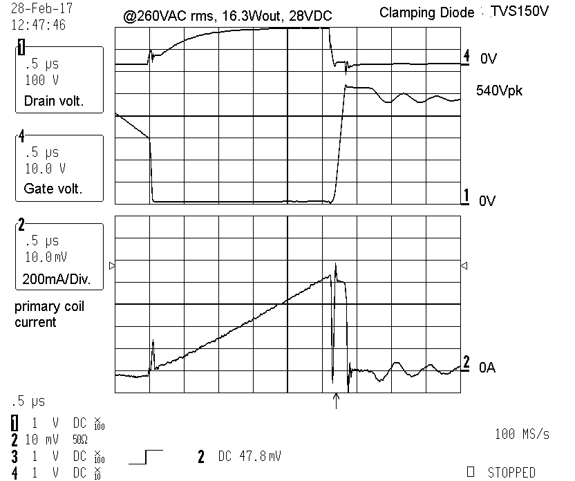
| With
the TVS150 only, Drain peak voltage reduced to 540Vpk, reduce
voltage stress in the MOSFET and would improve EMC. Much power in
clamping diode. Gate voltage rise up slow for a slow MOSFET Switch-ON, there is no need to switch on fast, because Drain voltage and Drain current is low and therefore no Switch-ON loss. Gate voltage rise-down for a fast MOSFET Switch-OFF, there is a need for a fast switch off, to keep switching loss in a reasonable limit. |
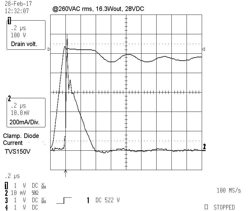
| @260VAC rms | @260VAC rms | @85VAC rms | @85VAC rms | |
| Drain pk voltage | Clamping Diode pk Current | Drain pk voltage | Clamping Diode pk Current | |
| TVS150V+TVS150V in series | 680Vpk (Figure 73) |
0.34Apk (Figure 73) |
425Vpk (Figure 72) |
1.7Apk (Figure 72) |
| TVS150V only | 540Vpk (Figure 80) |
1.2Apk (Figure 79) |
310Vpk (Figure 77+78) |
2.2Apk (Figure 78) |
| The harder clamping reduce the MOSFET voltage stress, transfer power to the Clamping diode. Propably will improve EMC. |
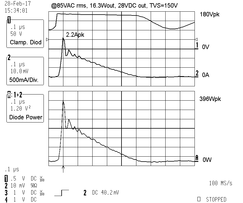
| Clamping
Diode TVS150V, voltage and current waveform. Diode peak power 396Watt
pk. Peak Power to much for repetitive clamping function, require PCB
heat-sink under repetitive 396Wpk. |
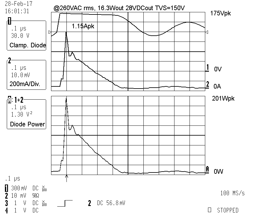
| Clamping Diode TVS150V, voltage and current waveform. Diode peak power 201 Watt pk. |
| @260VAC rms | @260VAC rms | @260VAC rms | @85VAC rms | @85VAC rms | @85VAC rms | |
| Drain pk voltage | Clamping Diode pk current |
Clamping Diode pk power |
Drain pk voltage | Clamping Diode pk current |
Clamping Diode pk power |
|
| TVS150V+TVS150V in series |
680Vpk (Figure 73) |
0.34Apk (Figure 73) |
128Wpk tp=0.05ms (no Figure) |
425Vpk (Figure 72) |
1.7Apk (Figure 72) |
528Wpk tp=0.1ms (no Figure) |
| TVS150V only | 540Vpk (Figure 80) |
1.2Apk (Figure 79) |
201Wpk tp=0.2ms (Figure 83) |
310Vpk (Figure 77+78) |
2.2Apk (Figure 78) |
396Wpk tp=0.2ms (Figure 82) |
| Two series diode sharing power. With higher clamping voltages, pulsewidth become smaller. Choosing the right TVS value a game of power distribution and EMC. |
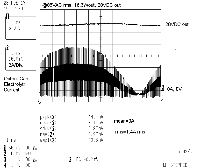
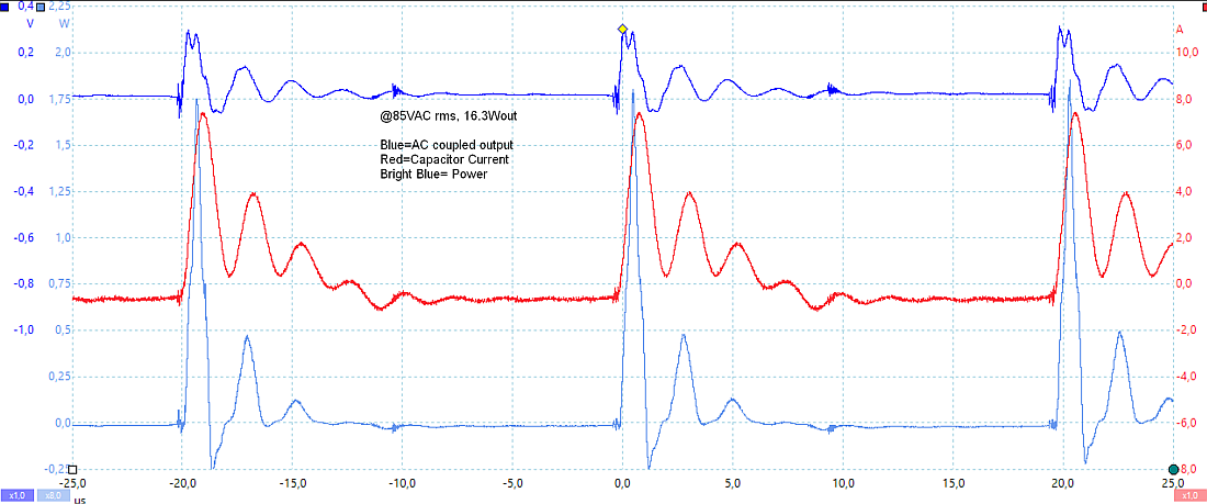
| Current
waveform of the output electrolytic capacitor, 2200µF/50V. Rms
current creates capacitor heating. Stay well below maximum limit to
prevent capacitor from heating-up - will increase capacitor lifetime. Here 1ms/Div. * 10 Divisions = 10ms, that is exactly 50Hz*2 =100Hz exactly one cycle ==> therefore rms and mean value correct for the setted oscilloscope timebase. Mean must be zero, same amount of In and Out capacitor currents. |
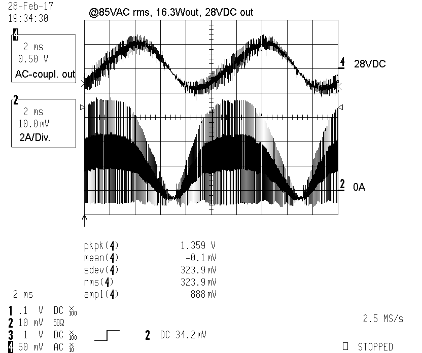
| AC coupled output voltage, 1.359 Vpkpk. 100Hz ripple plus switching frequency ripple. |
|
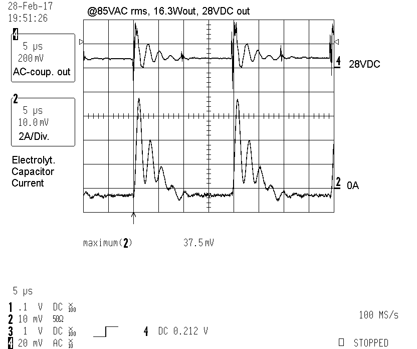
Switching Current Ripple into the
Electrolytic Output Capacitor 37.5mV*2A/Div. = 7.5A pk.
AC-Switching-Ripple voltage approx. 180mVpk
Resistance = 0.18Vpk / 7.5Apk = 0.024 OhmEquivalent Series Resistor (ESR) = 0.024 Ohm @ f=100-500kHz Capacitor Datasheet value = 0.019 Ohm for 25°C, 100 kHz Measurement fits well to the Datasheet value, consider also the real measurement has PCB wires, solder junctions and a inductive current loop wire added to the measurement - both values fitting excellent to each other. |
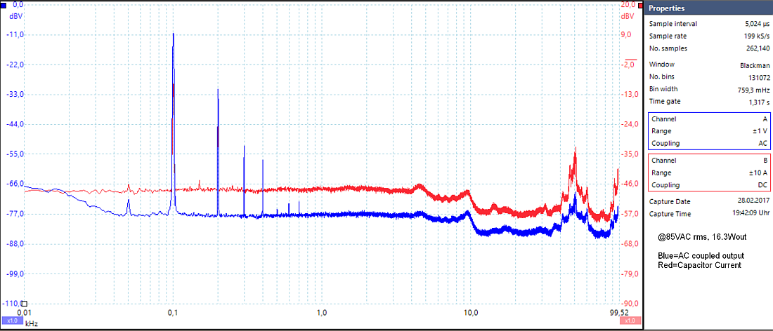
| FFT Spectrum of Capacitor current and voltage, Span 10Hz to 100kHz. What we see here? small 50Hz (mainly transfered by air) very large 100Hz (AC-rectified Ripple) 200Hz-800Hz (AC-rectified harmonics, AC line harmonics) 50kHz (switching frequencies starting here) 100kHz (second switching harmonic) |
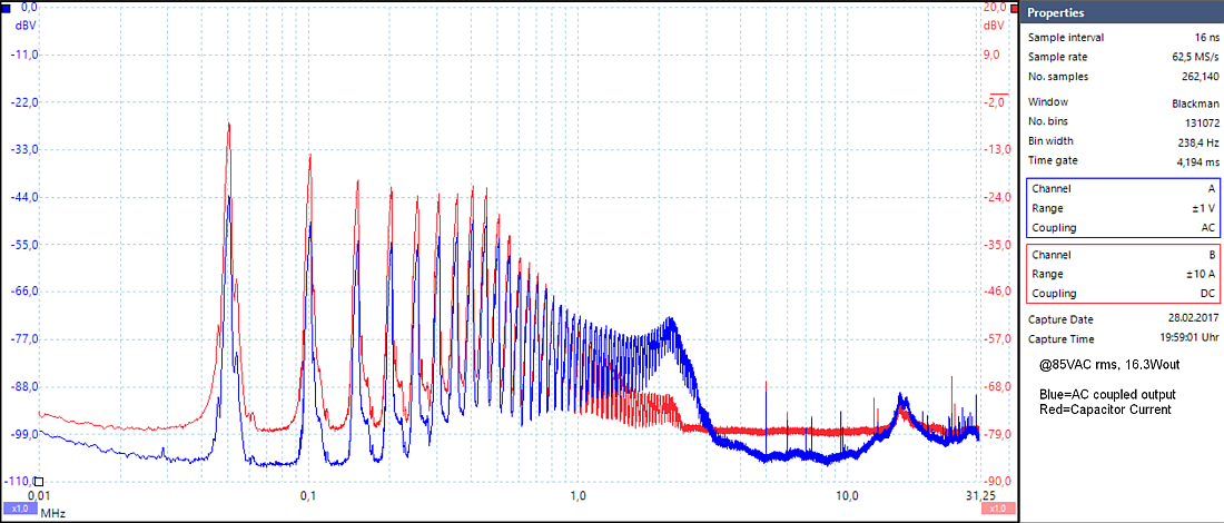
| Span 10kHz to 30MHz, we see 50kHz-2MHz (switching frequencies) Blue Capacitor voltage curve shows a significant pole, capacitor impedance rise up at 2MHz. Caused by capacitor+Layout.
Output clean in higher frequency areas. Used oscilloscope a 200MHz/12Bit resolution oscilloscope, 1Meg Inputs. |
| Power heating up the capacitor. Difference between ohmic thermal power and LC-power doesn´t matter here. Any DC-offset in the current probe and ADC-input offset voltage will create an additional measurement error. |
|
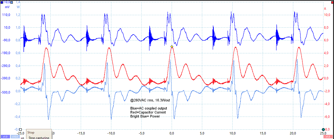
With 260VAC rms, voltage and current waveforms looking quite different
compared to 85VAC rms. Capacitors has less peak power, but more often.
|
|
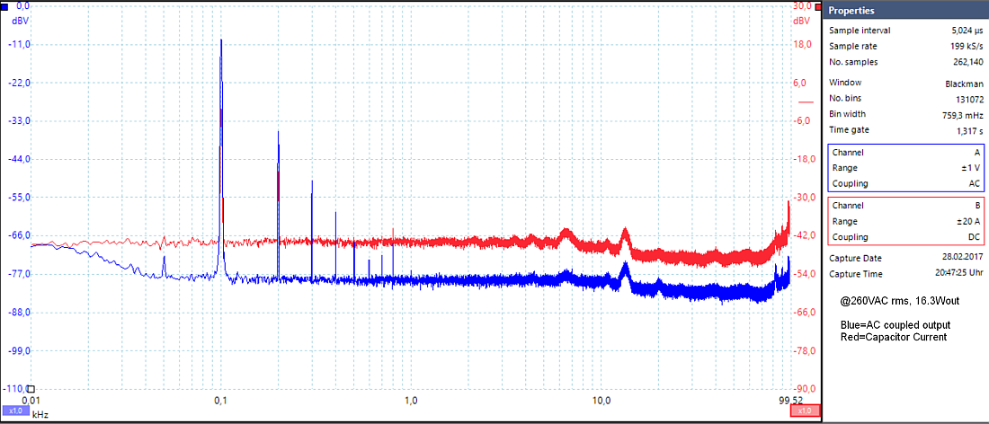
With 260VAC rms, voltage and current spectrum looking different
compared to 85VAC rms. That means EMC tests should be done under different AC line voltages.
|
 .
.