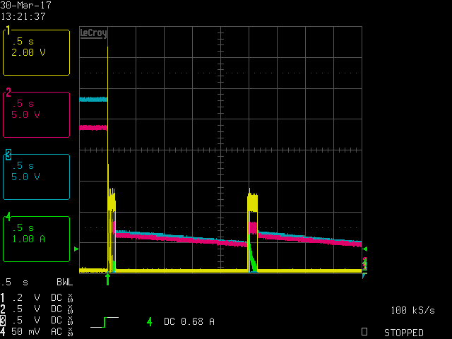
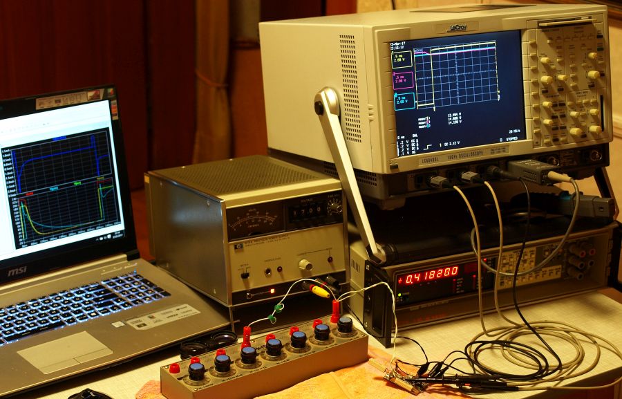
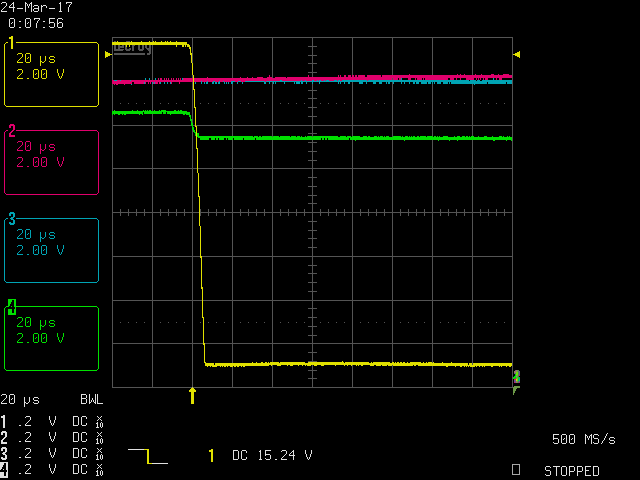
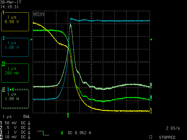
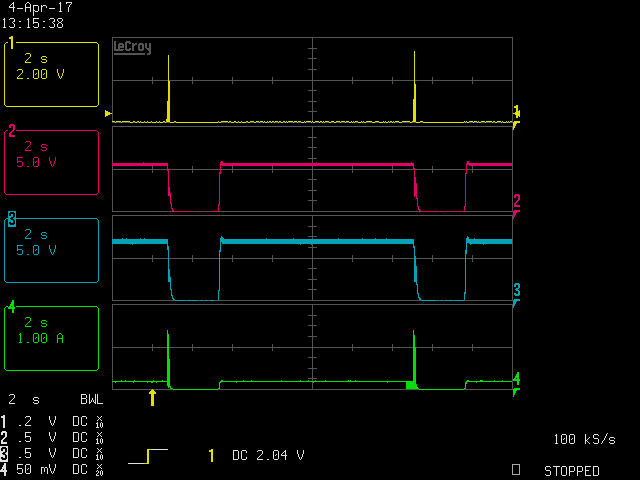
| It
is necessary to develop a small circuit running with the PFC.
Unfortunately I can`t show the purpose of this circuit, please don`t
expect an explanation for the purpose of the circuit. working on the isolated 28V low voltage secondary side, no risk to use now a more comfortable oscilloscope with lower maximum input voltage range. Note the labtop, measure and simulate at the same time, a good method to develop a circuit. |

|
These are the things you should have to solder SMD PCB`s and prototypes.
From left to right:
With the hot-air tool it
is easy to solder the small copper-PCB-pieces on the ground
plane, it is like placing a SMD part. Whitout an hot-air tool use e.g. fast
2K-Epoxy-Glue - but be aware glued copper-pieces remove accidentially
sometimes, possible fix them with a large soldering iron (not
easy, little tricky). Easiest, solder them with the hot-air tool.
Soldering on a real wooden table and chair (hard-oil furnished or natural, no plastic paint) - no further need for ESD protection. Wooden floor (hard-oiled or natural surface), 100% wooden chair and use 100% cotton clothes - avoid all plastic and synthetic in the working area. Natural cotton and wood under high relative humidity (no drying air-conditioning) is in general a safe ESD condition for almost all parts. Of course very sensitive parts like laserdiodes and high impedance HF electronic require special ESD environmental and handling procedures better than the protection shown on the photo. It is possible to handle such also very sensitive devices under hobby conditions - but think very well what you are doing, each movement of your hand and your body has to be considered. Best read a physic book about electrostatic, you must understand first in detail why things are charging before understanding ESD protection. |
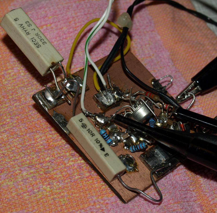
In my opinion, soldering a circuit direct on copper is an efficient method developing a circuit:
In my opinion disadvantages of the following methods developing a circuit:Breadboard with springs and flexible wires:
Prototyping PCB`s with stripes and holes:
Selfmade protoyping PCB`s with etching or milling machines:
Manufactorer Evaluation Boards:
Developing the circuit on the first Proto-PCB delivered to a customer:
The worst item for all these methods:"difficult probing" - often results in NOT testing an node.
Ein kleiner Gruss an die deutsch sprachigen Leser:
zweifelt an Methoden, wie: "zur Evaluierung einer Schaltung müssen alle Drähte und Bauteile gerade verlegt sein oder im 90° Winkel". Bei diesen Methoden wird dann suggeriert, dass das sogenannte "ordentliche Arbeiten" sehr wichtig ist, die eigentliche Aufgabe eine gute Schaltung zu entwickeln tritt dabei vollkommen unbeachtet in den Hintergrund. Die "sogenannte Sauberkeit am Arbeitsplatz" ist für die Entwicklung einer Schaltung einer der unwichtigsten Punkte überhaupt. Ist es bei mir zu Hause dreckig? - ich bin mir sicher - nein. Viel wichtiger hingegen ist die "Sauberkeit auf der PCB", insbesonders eng aufgebaute PCB`s leiden unter diesem Punkt, der Luftaufbau hat an diesem Punkt keine Schwierigkeiten. Eine total mit Flussmitteln versiffte Test PCB, ist in der Regel ein Beweis dafür was die Schaltung taugt: - wenig - außer viel Siff darauf. Wurde die manuelle SMD Prototypen Schaltung komplett unter dem Mikroskop gelötet mit gutem Licht, Flussmittel und Lötausstattung - wenn ja prima - oder erfolgte die Lötung unter Plastik Leselupen, Kopflupen oder sonstigen optisch dürftigen Hilfsmitteln? Die Preise selbst für ein gebrauchtes Stereo Mikroskop sind erträglich. Aussagen wie: "ich habe gute Augen" - zeugen von nicht verstandener Notwendigkeit. Selbst die schärfsten Augen sind einem Mikroskop um Längen unterlegen. Verheerend ist die Fehleinschätzung der Ansicht zu sein, stets alles theoretisch vorab entwickeln zu wollen - ohne Test direkt in die Serie hinein. Woran erkennt man sofort auf einen einzigen Blick innerhalb von wenigen Sekunden eine schlecht dimensionierte, meist auch nicht gut funktionierende Schaltung? An der Art und Weise wie der Schaltplan gezeichnet ist.
Die Mühe und die Verständlichkeit, die sich jemand gibt einen Schaltplan zu zeichnen ist das Spiegelbild zur schaltungstechnischen Qualität. Es spielt keine Rolle ob Handzeichnung oder CAD Tool, von Interesse ist das Erkennen des Willens die Schaltung einem anderen so zu präsentieren, dass dieser mit dem geringstmöglichen Aufwand an Zeit eine Chance hat die Schaltung zu verstehen. Wenn man Gelegenheit hatte den Schaltplan einzusehen, weiß man in den meisten Fällen innerhalb von Sekunden alles weitere über Schaltung und Dokumentation. |
|
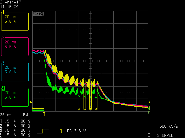
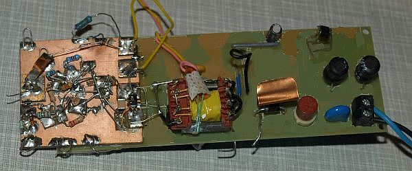
Board after finishing this pre-development level. - Ready to go for the first PCB layout - Eval Board looks now quite
different to it´s original condition. A full development of a
circuit require special methods, in my opinion, build up the circuit on
a self made evalboard, after knowing all voltages and
currents start with the first PCB.
This application note for the pre-development stops here with Part 8. Operates excellent now, final layout will be easy, without any unwanted surprising or time delay. END
|
 .
.