|
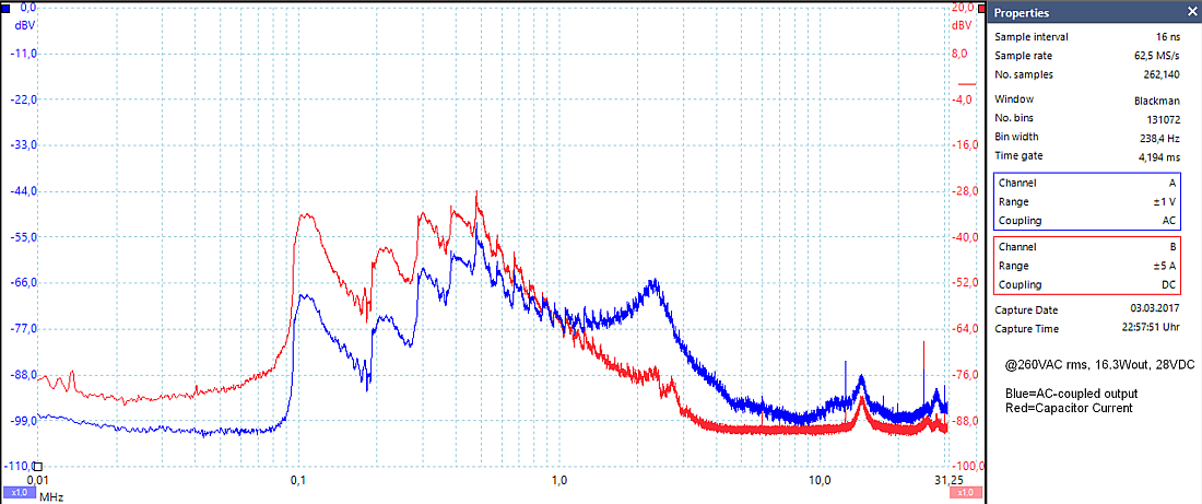
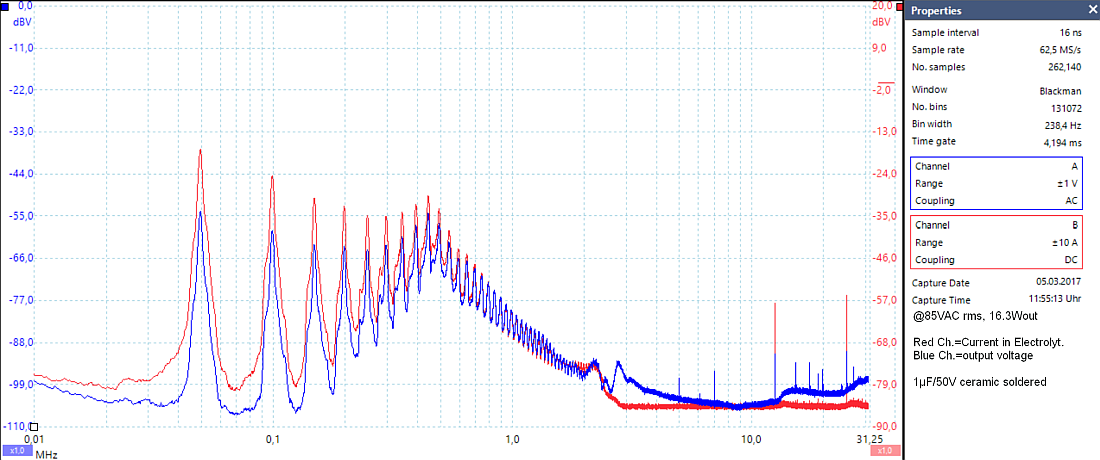
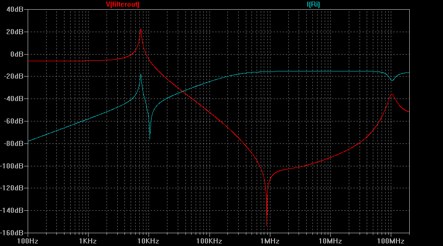
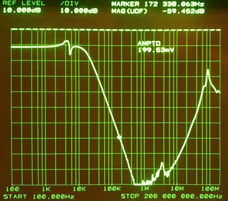
Span 10kHz to 30MHz, we see
switching frequencies starting 100kHz (wide spreading) Blue Capacitor
voltage curve shows a significant pole, capacitor impedance rise up at
2MHz.
|
| 85VAC rms | 260VAC rms | |
| AC-coupled output & Capacitor Current |
|
|
| EMC test should be
done with low 85VAC rms, normal 230VAC rms and at maximum voltage. |
| line current @85VAC
rms. Waveform from the supplying
safety transformer looks similar, sharp needles near zero created
by the DUT. |
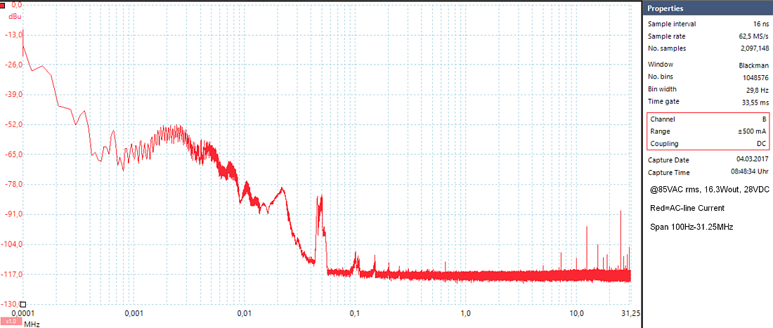
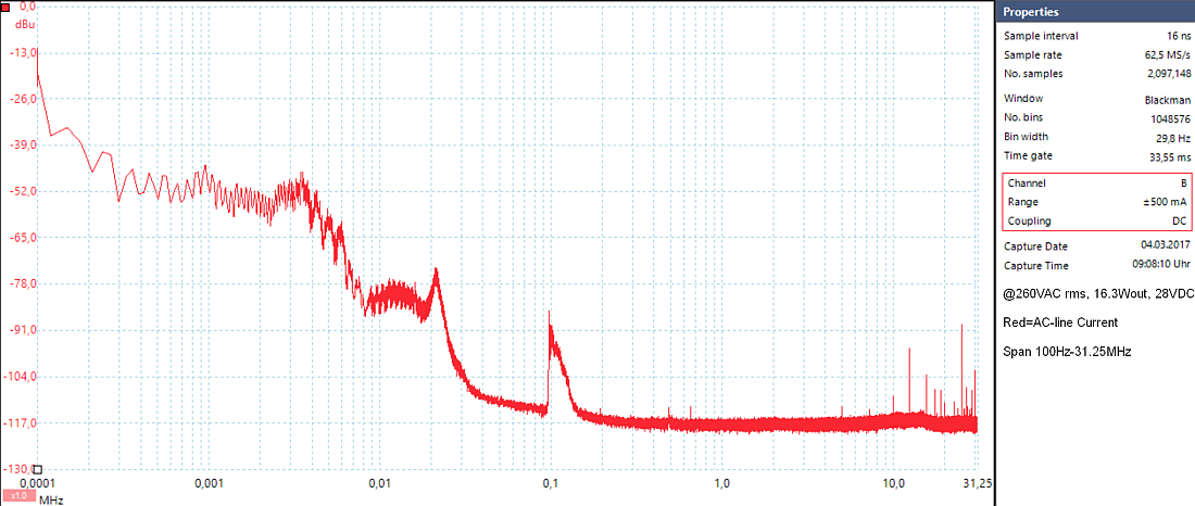
| Span 100Hz to 31.25MHz Switching frequencies at 50kHz. |
|
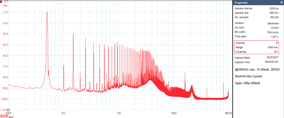
Span 10Hz to 100kHz The odd line harmonics are dominant. A perfect PFC would show only a single 50Hz frequency - impossible. |
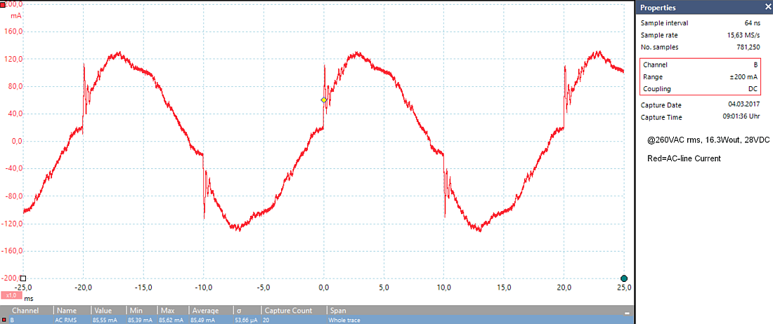
| @260VACrms. Sharp needles still significant. |
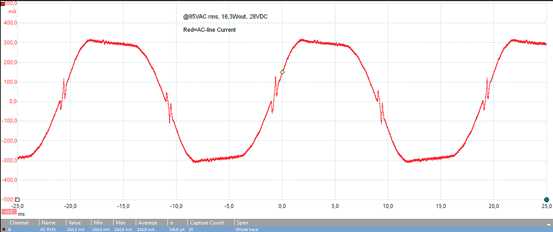
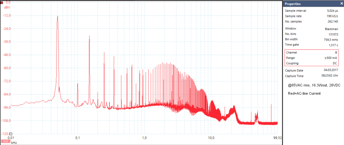
| @85VAC rms, AC-line current (line side), Switching frequencies at 100kHz |
| @260VAC rms, AC-line current (line side), increased distortion. |
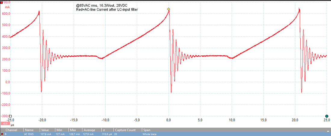
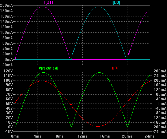
| Line current after input LC filter. Looks similar to rectified primary
coil current. Core in saturation under max. amplitude. |
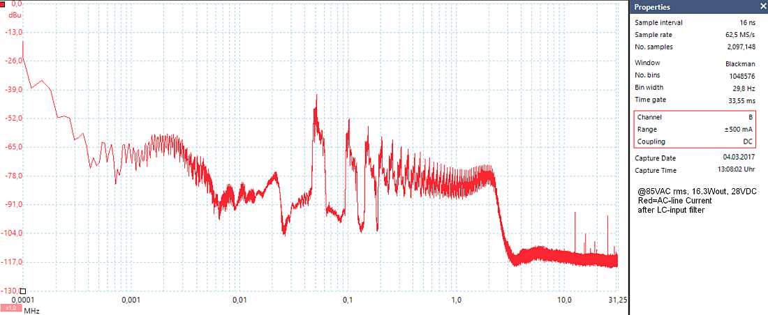
| Input line current after LC filter, compare to Figure 97. |
|
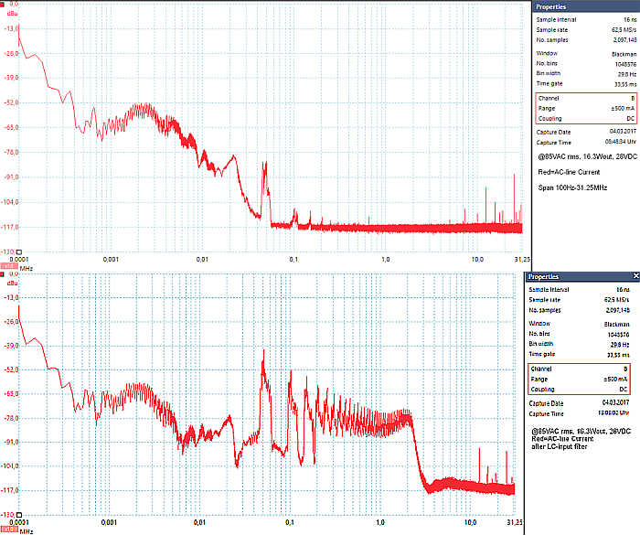
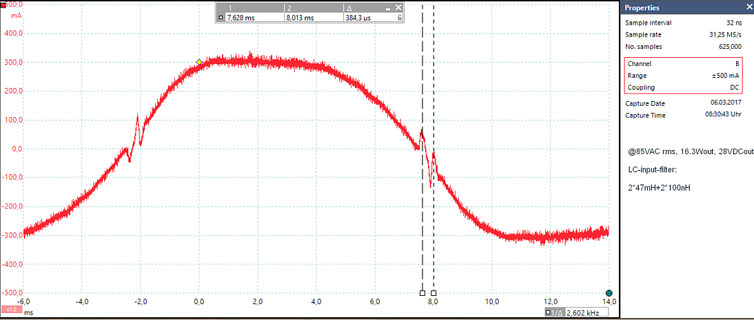
@85VAC rms, 16.3Wout. Both diagram under same scaling and conditions.
Filter removes unwanted switching
signals.
|
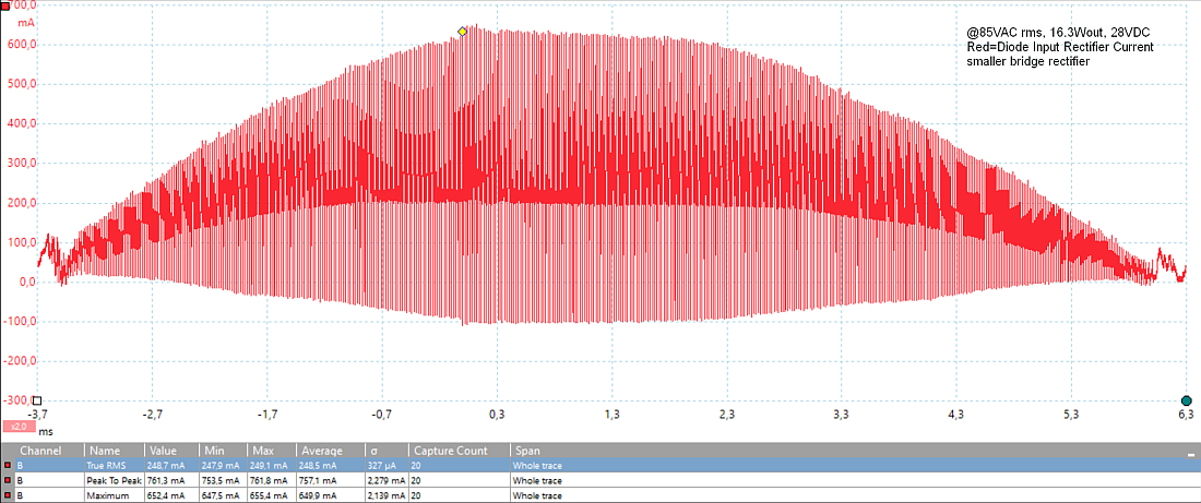
| Using a smaller package for saving board space. @80VAC rms -True RMS for a half sine wave = 290mA rms. @85VAC rms -True RMS for a half sine wave = 250mA rms. @105VAC rms -True RMS for a half sine wave = 210mA rms. @160VAC rms -True RMS for a half sine wave = 140mA rms. @230VAC rms -True RMS for a half sine wave = 100mA rms. @260VAC rms -True RMS for a half sine wave = 92mA rms. Rectifier is within absolute maximum ratings under all conditions. 85VAC rms cause highest input currents. Part require PCB copper for cooling, recommended. Consider lowest AC-line voltage and highest operating temperature. Absolute Maximum Ratings: max. 500mA rms @ Tc=25°C max. 300mA rms @ TC=80°C |
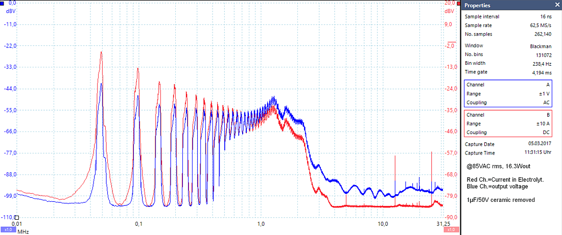
| 1µF/50V ceramic removed from output |
| 1µF/50V soldered to output |
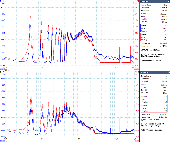
| Figure 106+107, 1µF soldered direct on output,
improves output spectrum. Both measurements done with the same
settings. Capacitor useful, because a post added linear voltage
regulator is in general not able to rejects higher frequencies.
Capacitor prevents post electronic from higher frequencies. |
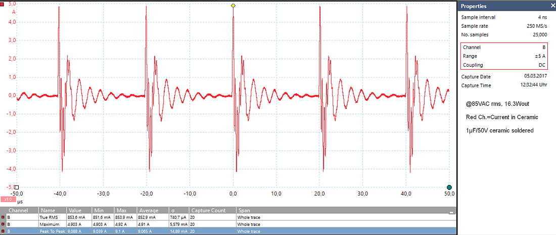
| Current
in 1µF, 5A peak Under higher frequencies the
electrolytic capacitor already behaviours as inductor and becoming useless for higher frequencies. Capacitor can be enlarged to 1µF-4.7µF, check datasheet for max. allowed peak and rms currents. Capacitor operates on a max. 16.3Wout power source, in case of cracking and shorted ceramic, danger - overheat or in worst case fire. Use a capacitor series with high resistance after cracking ceramic, available under different names. |
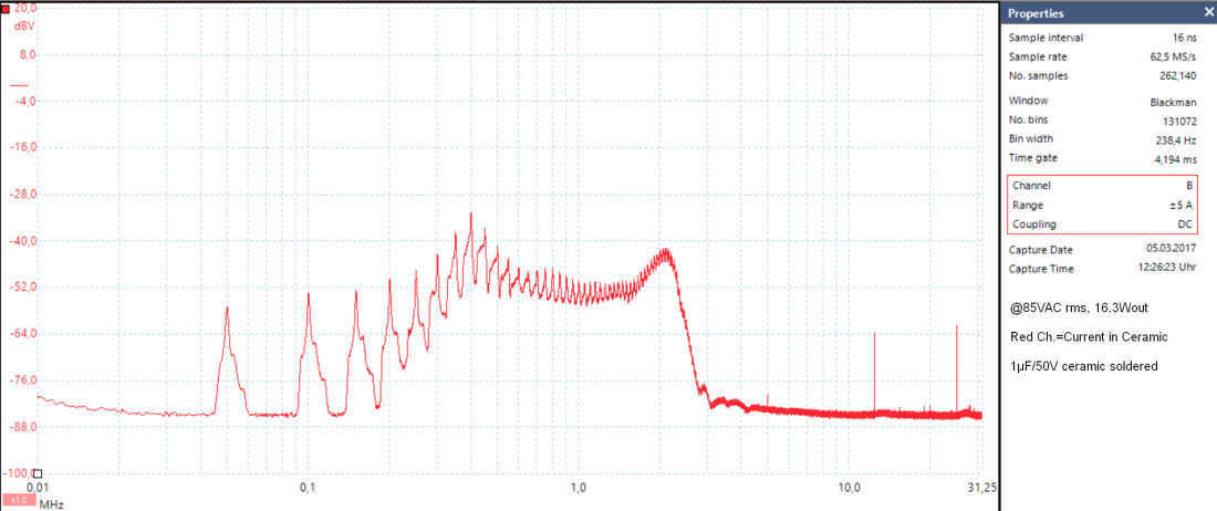
| spectrum in the current of the 1µF ceramic. |
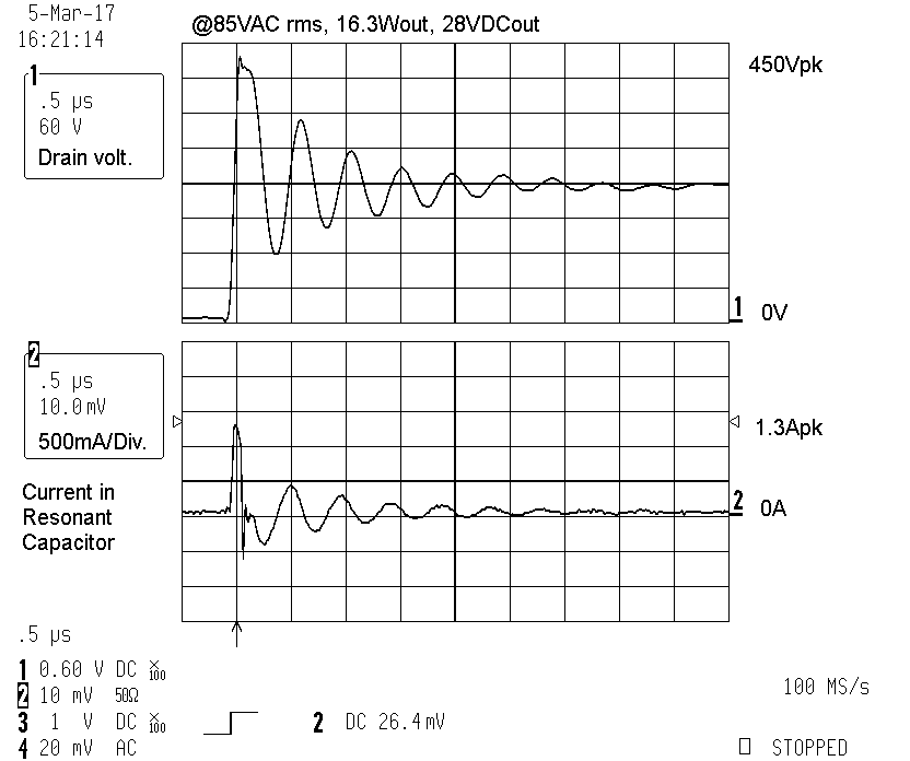
| 220pF/1kV COG capacitor peak current of 1.3Apk @85VAC rms |
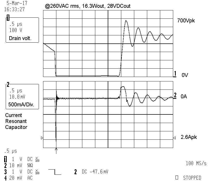
| 220pF/1kV
COG capacitor, peak current 2.6Apk @260VAC rms. Maximum peak under actice
clamping TVS diode at high Drain voltage conditions.
Consider max. allowed capacitor voltage and be carefull when doing
layout for enough distance between these high voltages. |
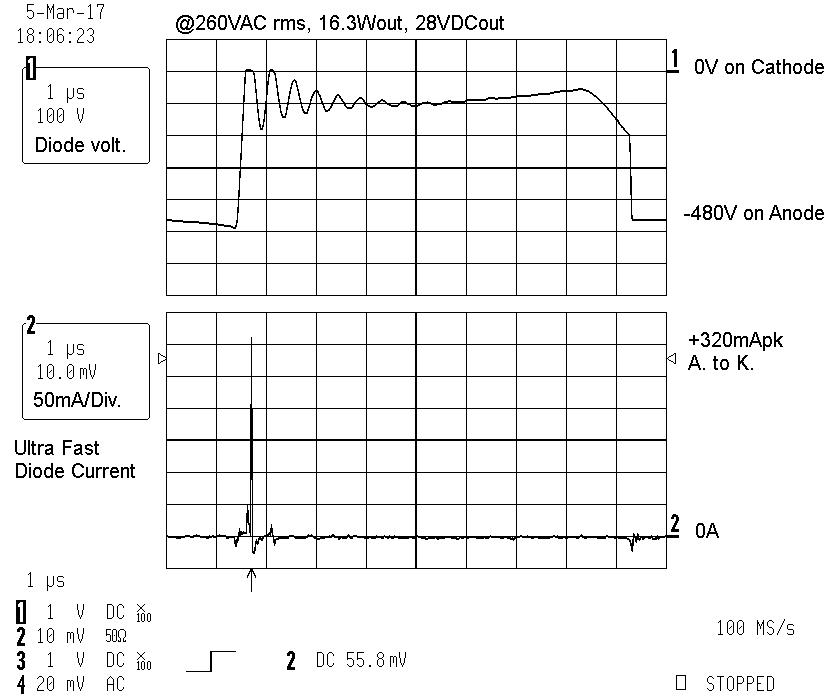
| Diode current and voltage, fast diode turn-on peak. Not EMC friendly, good for efficiency. Peak has a 40ns pulsewidth only. |
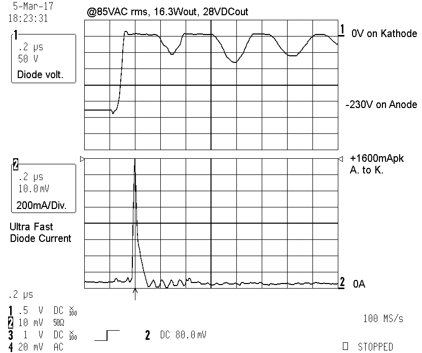
| Turn-on peak, current increased to 1.6Apk. Pulsewidth increased. |
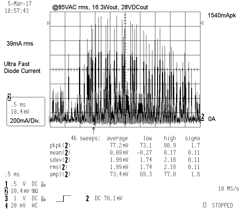
| Ultra fast diode current, 39mA rms for one sine cycle. rms and peak below absolute max. value. |
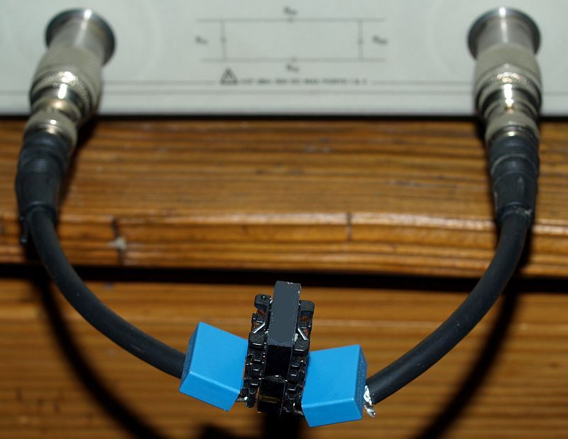
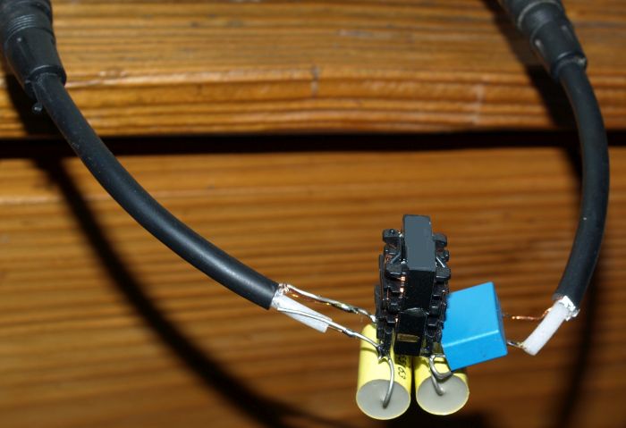
Photo shows the main parts of the line filter.
Main task of this filter:
reduction of the fundamental and the harmonics of the switching current.
This filter is important to reach a good powerfactor with the
target of an current waveform following exactly the waveform of the
input voltage. Filter reduce high-frequency components in the line
current, necessary for a EMC conform design.
|
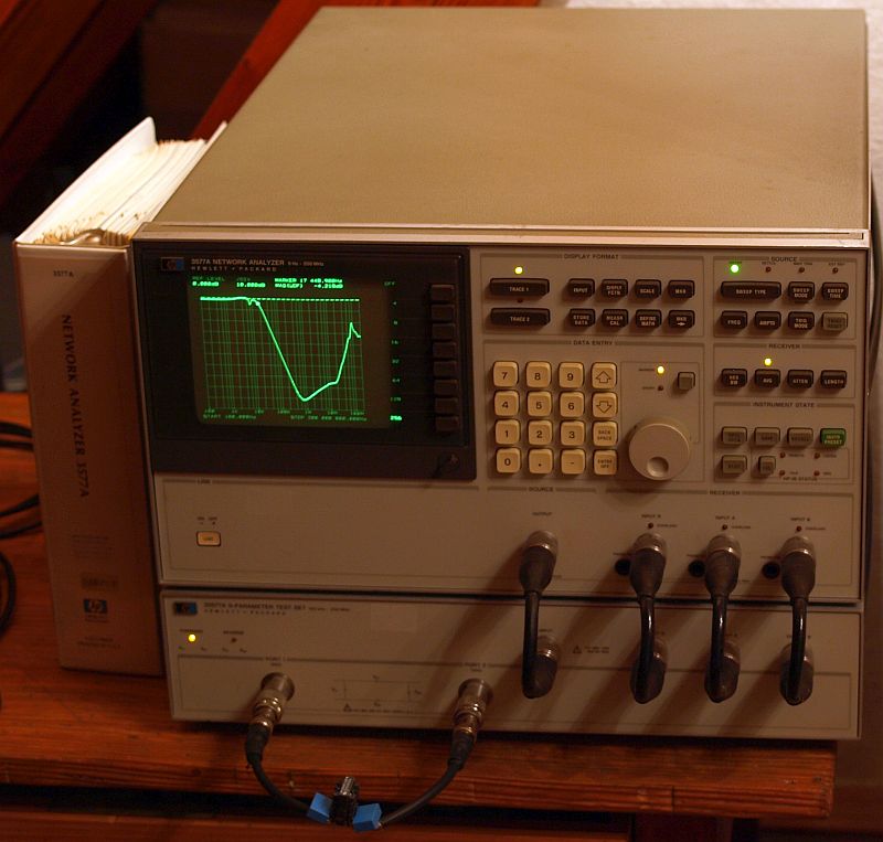
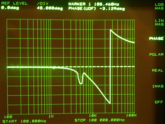
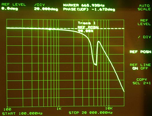
Network Analyzer 3577A together with 50 ohm S-Parameter Measurement Set
This network analyzer can
response the transfer function amplitude vs. frequency, if necessary
also the phase vs. frequency function (not shown here). All
S-parameter directions S11, S21, S12, S22 can be measured comfortable.
Forward and reverse direction - pressing only a few buttons. Measurement can be normalized for highest precision. |
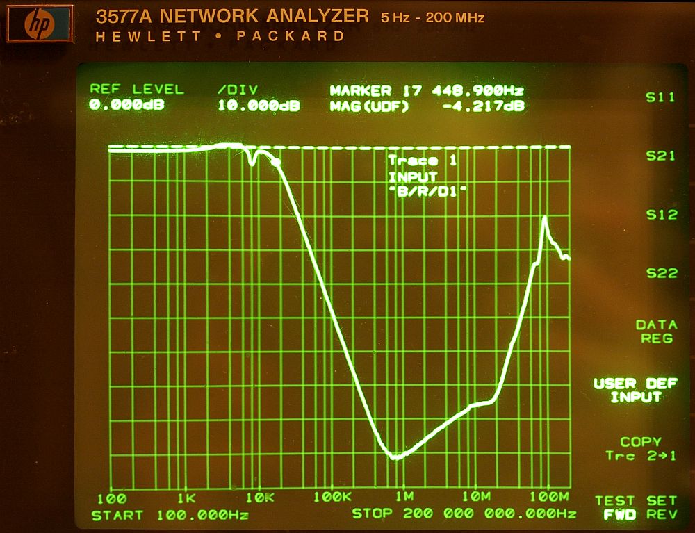
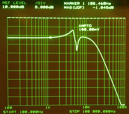
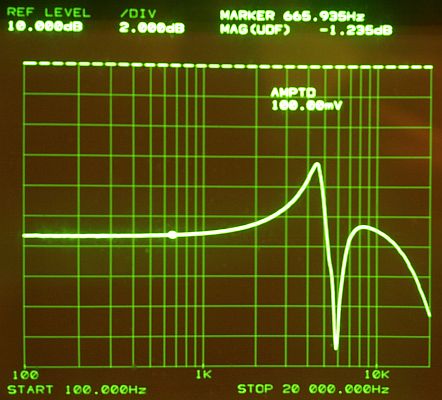
Filter amplitude vs. frequency
|
|
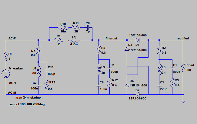
Trying to find a schematic for the network analyzer measurement.
The analyzer has a 50 ohm source impedance and 50 ohm load on the
receiving channel.
The inductor has two 47mH windings coupled on the same core. I guess as coupling factor 95%. On both sides of the double-coil are 100nF foil capacitors. The network analyzer short one winding. Coil has 47mH for currents flowing both in the same direction, these are not the operating currents, 47mH effective for common mode signals, today I found no way to measure the network for common mode with the analyzer. Input and output are on the same ground.
|
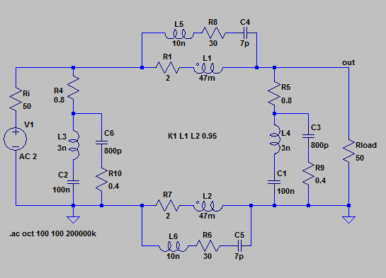
| Simulation result of the circuit in figure 119. |
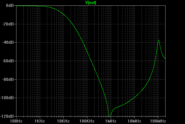
| Measurement and Simulation in comparison. There was no way to force the simualtion to create the overshooting near 3kHz, needs further investigation. Coils are difficult under simulation, non-linear parts over frequency and current. |
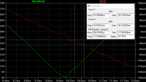
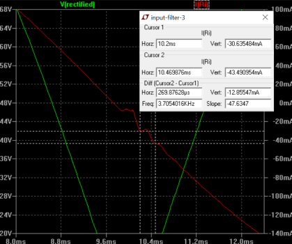
| AC-line current shows a waveform distortion of 2.6kHz - why? |
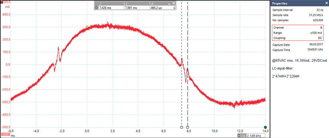
AC-line current waveform distortion of 2.1kHz after changing from 100nF to 220nF
|
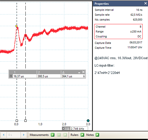
| AC-line current waveform
distortion of 2.7kHz after changing from 100nF to 220nF @240VAC rms. |
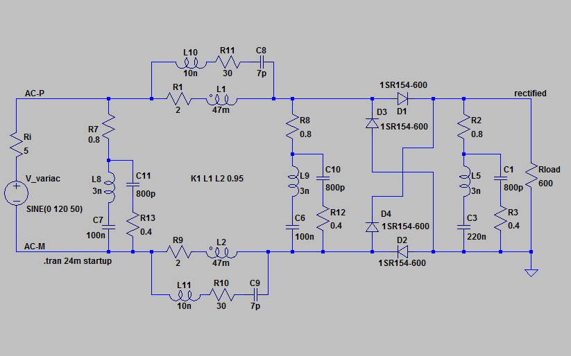
| Simulation of the input filter with post bridge rectifier. If 100nF or 220nF build-in no matter much. |
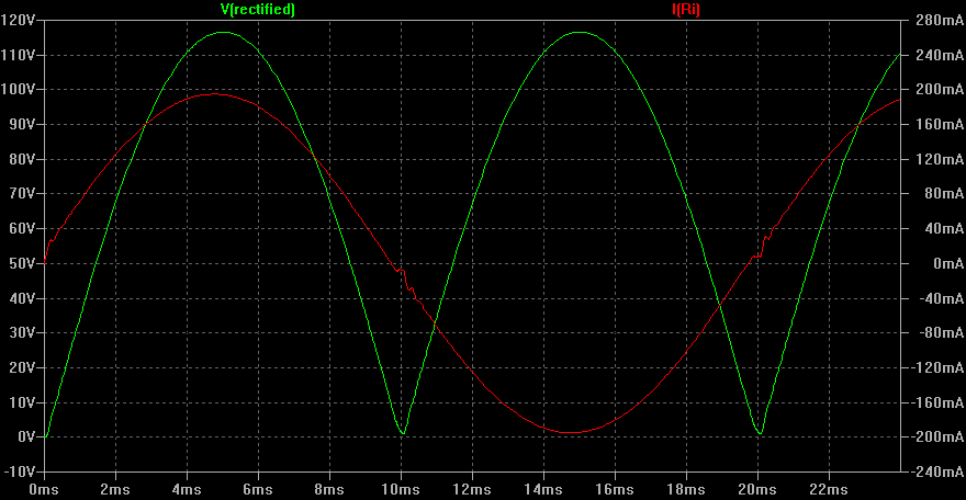
| Generator current shows Peaking AC-line distortion, similar to the measurement. |
|
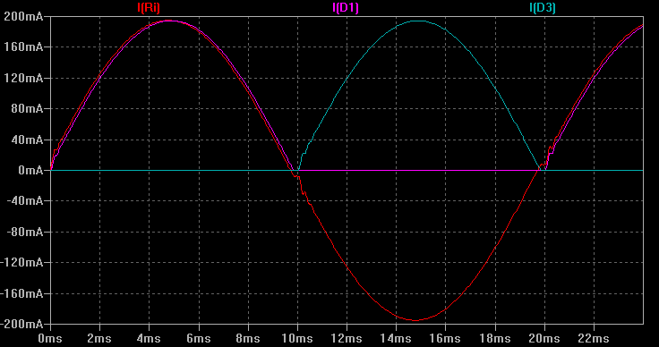
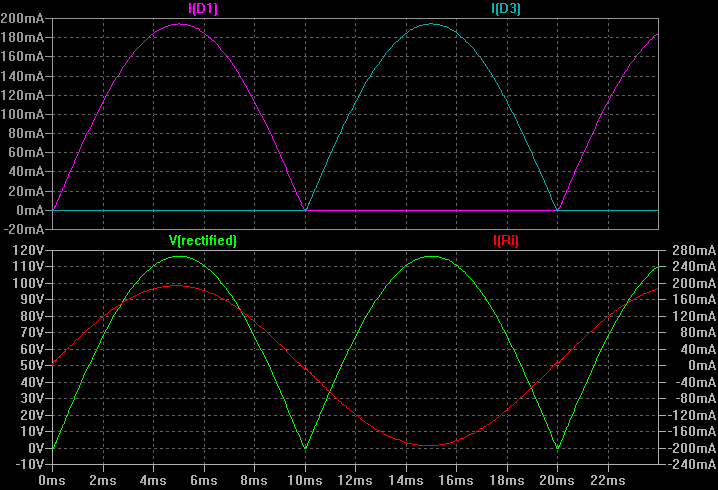
Distortion in all Diode Currents.
Diode i vs. u curves are not ideal, 0.7 volt deadband. Zero area highly
nonlinear with fast changing currents and voltages, resulting in
stimulus under many frequencies, powers LC-circuits powered and
oscillation starts if not damped.
|
|
Inductor had common 2*47mH with a
coupling factor of 95%. Let us remove the 95% common inductance and
calculate the leakage capacitance:
5/100 == x/(47mH+47mH) ==> x=(5/100)*(47mH+47mH) ==> x=4.7mH leakage inductivity.
The effective lowpass filter for the AC-line distortion created by L1=4.7mH and C3=220nF. |
|
Distortion back with stray inductance 4.7mH & 220nF, same frequency compared to figure 127
Distortion caused by - capacitor on the rectifier output plus serial inductance. This is the way back to the traditional 50Hz Transformer ==> Bridge Rectifier ==> large Electrolytic, resulting in the common known terrible peaking AC-line currents. When increasing C3 and playing togehter with L1 all these effect can be seen. Sometimes when obeserving an unknown effect you can`t explain, try to amplify the effect, sometimes a way for a better understanding. |
|
Plot based on circuit figure 130
This is the result I want to see.
Here is the missing unexpected peak in the amplitude response, below
10kHz. Changing a litte the coupling factor/leakage inductance
and peak frequency change a lot. Second order LC lowpass with
high quality factor and 20dB peaking. Damping is low in this
simulation, generator impedance low.The nonlinear rectifier diode i vs. u curve behaves like a heavyside function with a wide range of stimulus frequencies. Filter response with AC-line current distortion. Final result a decreased powerfactor - the main purpose of an powerfactor controller IC. As mentioned before it is difficult to design an input-filter. Peakfree LC-filters without damping resistors are not possible. This filter design has just started now. Remember again my four rules for a better design (from Part 2): "Best developments methods consider these important issues:
Do you have all necessary test equipment in your lab, NO? Hobbiest: if no - understandable, expensive, not important in your life, electronic just for fun, no need, ok. Commercial: if no - yo waste a lot of money - for not understanding your products in detail, using much time seaching for errors in a faulty design. Many engineers and 50% of "deciding people" do not understand what´s important. Do not spend long with them about this topic - it´s a waste of time. Search for the other half and talk with them, a greater pleasure. Thank you for reading part 1 - part 6. I´ve told you in the beginning of part 1, the story do not show a circuit. The story: how to design and learn which methods are important. This is your gain for reading all this long stuff: hoping you understand the four rules above. |
| LC
Filter modificated to 100nF (yellow) and 220nF (blue, after rectifier),
similar values as in Evaluation Board and in figure 130. |
| LC filter measured with 50 ohm source impedance, reduce amplitude peak compared to figure 130. Phase shift cause additional power factor distortion. |
 .
.