| Mesuring
now AC rms voltage with a true rms DMM, before was measuring with the
transformer neddle meter, not enough precision. When applying low 90
VAC rms under full load, supply switch OFF. Therefore increasing
current limit by a shunt resistor change. |
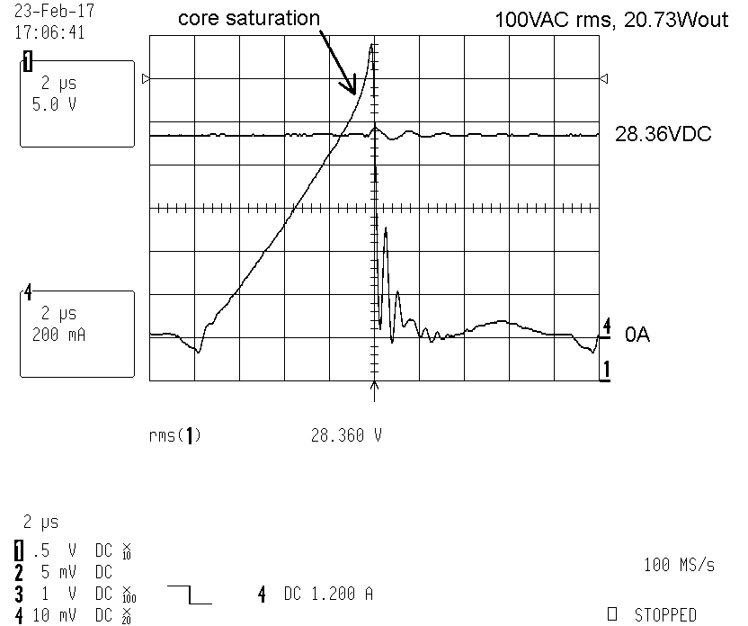
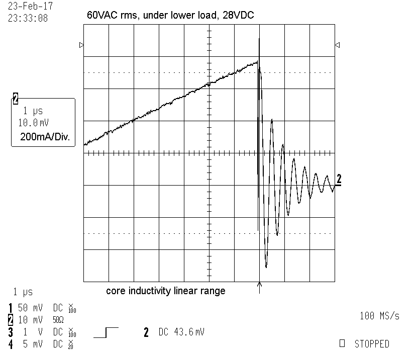
| Shunt
changed, now 20.7W load runs under 100VAC rms, with a lower voltage
Supply switch OFF. Lowest supply voltage requires the most current in
the primary winding. Core has reached maximum power, core become into
saturation, current rise very fast for high currents - core can not
store more magnetic energy. Further increasing current can damage the
circuit. Core becomes warm when supplied with 1.4A peak. Maximum load must be decreased for a save core. Reducing load to 16.3 Watt: minimum possible AC voltage = 85VAC rms @ 25°C, 16.3 Watt, 28VDC |
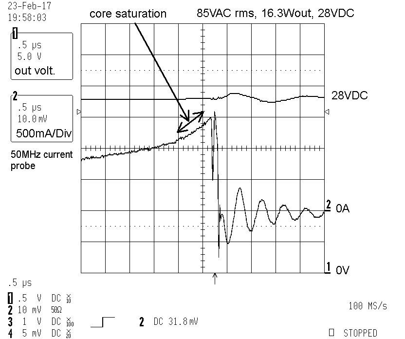
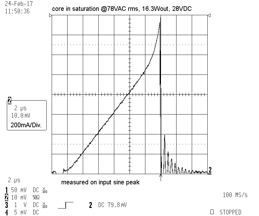
| Load
decreased to 16.3Watt, minimum 85VAC rms can be reached. Core close in
saturation. Consider this is room temperature, an additional ambient
temperature weaks the possible core saturation. Output voltage adjusted
close as possible to 28.0VDC. |
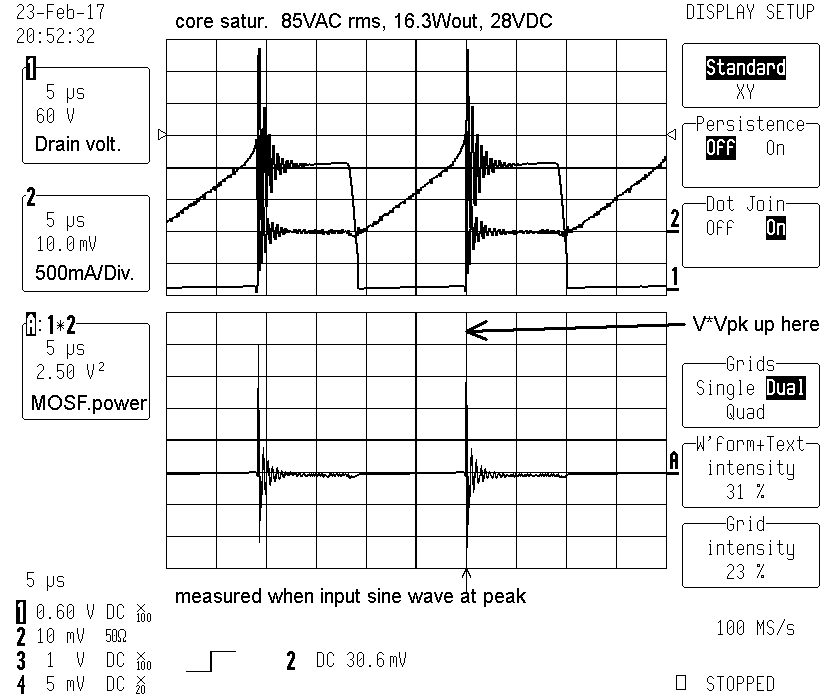
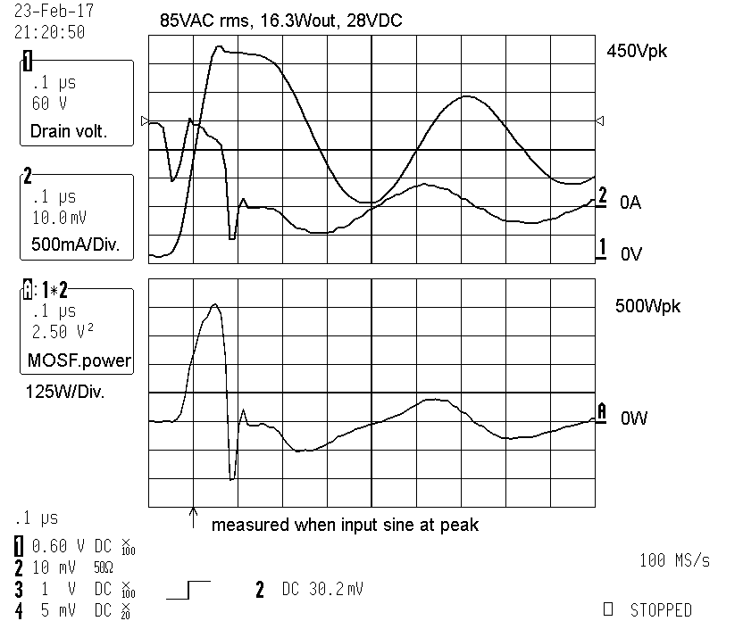
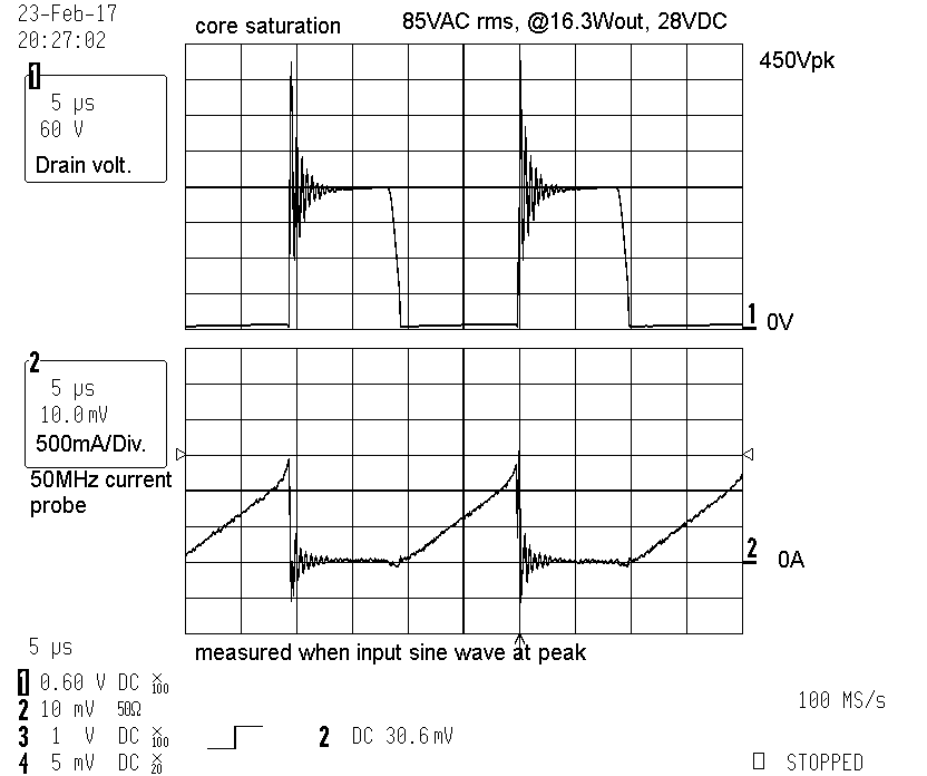 Figure 59
| Core saturates when input sine wave reach its higher voltage. Controller peak current detection approximately adjusted to 1,4A. It is possible to increase the peak current limit, but the rising current slope will increase further. Only the current will increase, but not the area under the current, the integral indicates stored magnetic energy - Increasing current, a good idea when integral can be increased, but when doing here only increasing current slope resulting in losses in core and MOSFET. |
| The current probe can not be recognized by the oscilloscope, different manufactorer, scale in volt/div. Channel 1 * Channel 2 = Channel A (Power) 1V * 0.01V = 0.01V² == 0.5W ==> 1V²== 50W When switching OFF the MOSFET there is a switching peak power of 10V² == 500Wpeak |
| Same measurement as Fig. 60, faster timebase. MOSFET peak power 500W for approx. 100ns. Energy: 500W*100ns = 50µ Joule (but more than 100000 times per second). This is an important parameter in the absolute maximum ratings, the used MOSFET has a 140µJ limit. If the designer decides to decrease the switching speed for a better EMC, keep the "Avalanche energy, repetitive" in consideration, I am not sure if this parameter is valid for both current directions, I think so. This measurement require good quality and fast probing. A fast scope with high sample rate an advantage. Would be an excellent task for a fast, high sample rate scope - some models with special power software options available. Ideal for a fast >8bit resolution model. Consider also, a fast 500Wpk can be a good and powerfull EMC source, when connecting to an well adapted arial - highest emission. Therefore it is a number-one-task in the layout for the Drain net, to create a "most bad adapted arial", keep most of the energy in the wires and prevent from radiating as electromagnetic wave. Drain voltage and Drain current are in 90° phase shift - LC oscillator. |
| a lower load, looks perfect. |
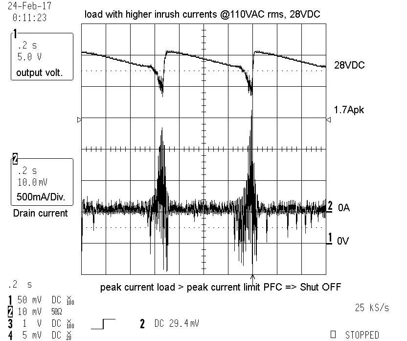
| An electronic load with inrush current. Controller detects high inrush currents for a Switch-OFF. |
| For a test purpose current peak limit has been increased from 1.4Apk to 1.7Apk. Core comes into more saturation. Not much gain on more magnetic stored energy, but highly increasing useless extra currents through the MOSFET, resulting in extra heat of core, winding and MOSFET - this is too much core saturation. |
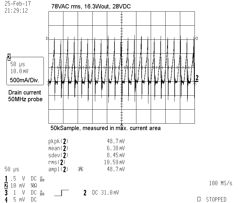
| Measuring
a maximum powered MOSFET. Current integrated in the area with the most
current. Controller Ipk level still set to 1.7Apk (saturation started).
rms value (both current directions, MOSFET+Diode) = 10.59mV = 530mA rms |
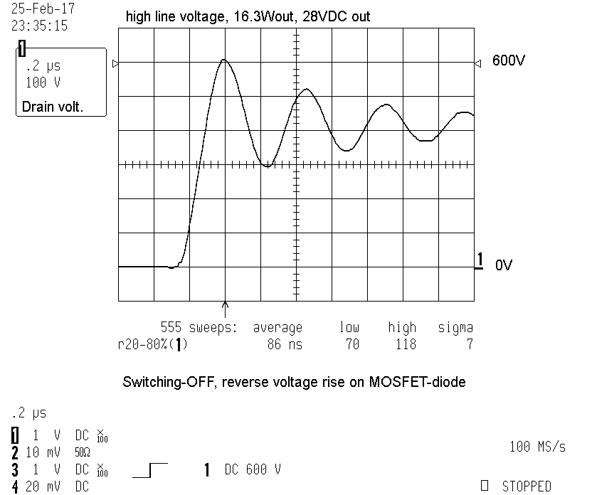
| Running
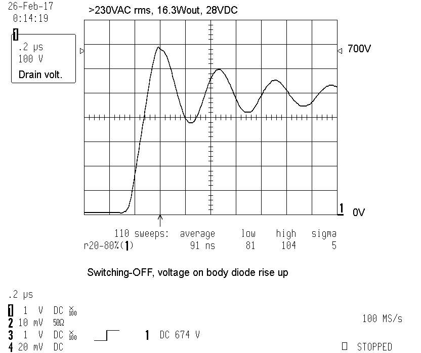
circuit under 230VAC rms. Measuring the risetime of the Drain voltage
when switching OFF. Scope set to a 20% to 80% risetime measurement, this means in Figure 66, the risetime mesured between 120V-480V. Deltavoltage 480V-120V=360V Slew-rate = 360V/86ns = 4.2V/ns, Datasheet absolute maximum rating: max. 50V/ns. |
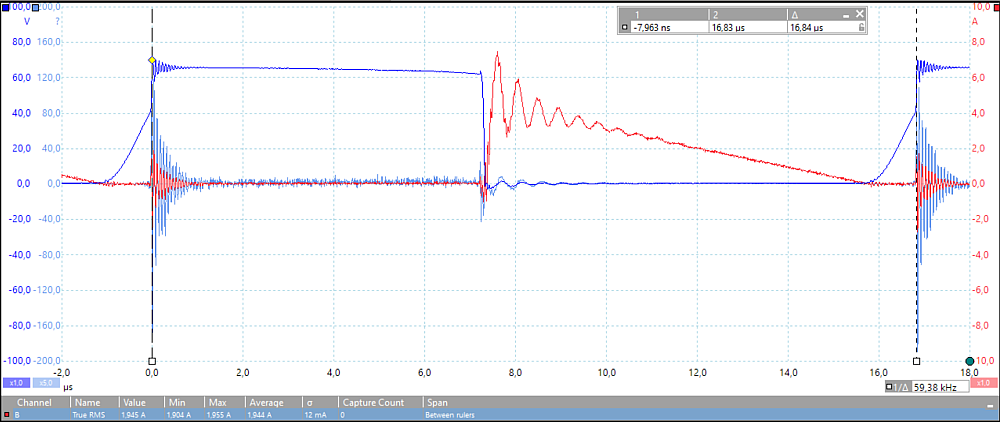
| Channel A (dark blue): Output diode voltage Channel B (red): Output diode current Channel A*B (light blue): Output diode power @115VAC rms, 16.3Wout, 28VDC True RMS Ch. B (current) = 1.945A rms for a cycle. Diode has 3A maximum average forward current limit. The 1.945A rms is a trustful value. Using here a 12Bit/200MHz oscilloscope, measures with more precision. Diode signals having a large dynamic range, from zero to high. Still a problem are any offset voltage caused by 50MHz current probe and voltage channel offset. The power calculation A*B, do not trust the values for highest precision, it is a good approximation, not more. Beware when using such special equipment: The risk using this 12bit scope, this type has only a specified max. +/-20 Volt input range, danger when working on a higher voltage power supply here. I don´t know at which voltage the input damages, not interested to know. Therefore using this scope only with a quality 1:100 probe, isolated current probe and doing only measurements had done before with another safer input scope. Necessary to think ALWAYS! at which potential the personal computer USB-ground actual connected. Never use such special equipment for starting evaluation under higher voltage circuits. Use them only after knowing exactly the magnitude of signals.
|
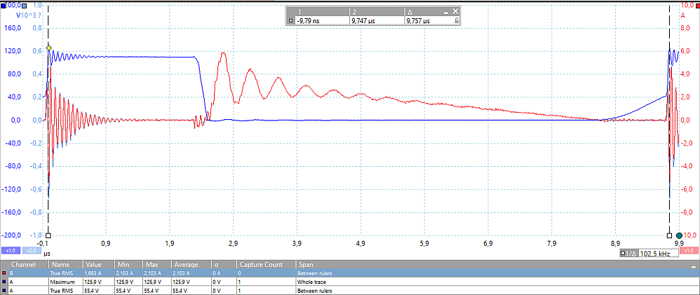
| Channel A (dark blue): Output diode voltage Channel B (red): Output diode current Channel A*B (light blue): Output diode power @258VAC rms, 16.3Wout, 28VDC Diode rms 1 cycle = 55.4V rms Diode max. = 125.9V Diode current rms = 2.1A rms At high input voltage: output diode voltage reach a maximum frequency rise Diode peak current decrease. Diode rms cycle current increase. |
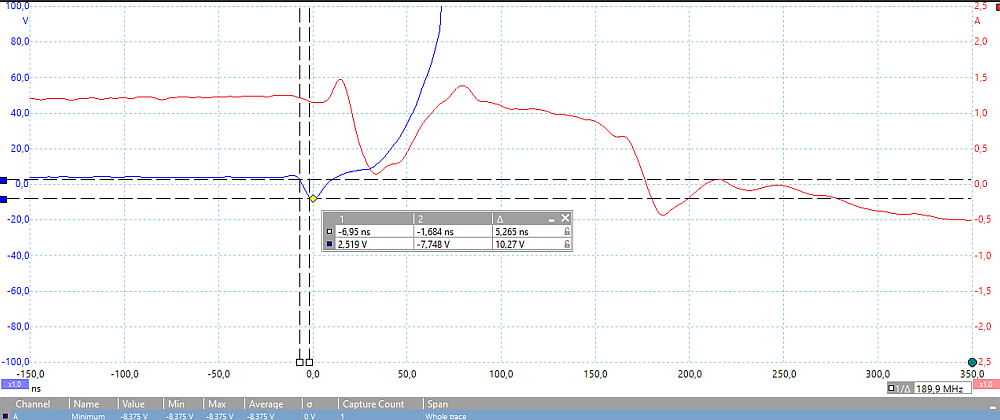
| Channel A (dark blue): MOSFET Drain-Source voltage Channel B (red): Primary winding current (Drain + parallel C-resonant-Capacitor). The real Drain current can not be measured, because parallel there is a 220pF Resonant Capacitor. For a real Drain current measurement, Evaluation Board should be prepared with a Drain wire-loop. @86VAC rms, 16.3Wout, 28VDC out Here the MOSFET diode becomes very fast conducting during MOSFET Switch-OFF. The recovery diode slope is the same falling and rising. The Flyback principle here use an unclamped inductive switching method resulting in fast voltage rise. Real drain current can not be seen, because of parallel Capacitor. Danger under a too fast voltage rise: internal parasitic Bipolar-Junction-Transistor can start conducting. In case of error, MOSFET becomes in ON-condition without applied gate voltage. Not yet understood here for me, needs further measurements. Measured Slew-rate under forward conducting body diode = -10.27V/5.2ns = -1.975V/ns Please consider here also the bandwidth of the Test Equipment:
A verification requires a faster oscilloscope and excellent probing. A good idea would be the use of a 500MHz or 1GHz scope together with a high quality 500MHz 1:10 or 1:100 passive probe. But it is a dangerous measurement for fast test equipment.
A fast Switching MOSFET is fine for a good power efficiency and space requirement, but has disadvantages in part reliability, part lifetime and EMC emmisions. Fast switching creates dv/dt stress on the MOSFET - not only heat cause stress on a MOSFET. |
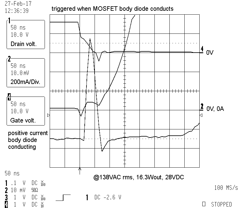
Current probe (primary coil) reversed.
Fastest Voltage slew-rate under reverse recovery: approx. 10V/40ns The oscilloscope should be faster for this measurement, 100MS/s single shot sample rate is not enough. But not a problem the quality can be observed. Problem with too fast du/dt ratings, internal parasitic BJT can become in an unwanted conducting condition, not observed here. Reading of MOSFET manufactorer application notes for explanation of max. du/dt and di/dt ratings required, measurement not yet fully understood for me. |
| Core saturation: keep available maximum output power low as necessary. Core saturation: depends on position within the input sine wave, search for the peak current. Core saturation: adjust maximum peak current @ lowest input voltage and @ highest ambient temperatue. Core saturation: Controller operating frequency too low, max. core power specified under higher frequency. Core saturation: Controller frequency can not increased, no setting possible. ------------------------------------------------------------------------------------------------------------------------------- Flyback: unclamped inductive switching (clamped at higher peaks by TVS-diodes). Flyback: cause high voltage V-drain-source stress. Flyback: low part count ------------------------------------------------------------------------------------------------------------------------------- Controller: fast MOSFET Switch-OFF, reduce MOSFET switching losses Controller: fast MOSFET Switch-OFF, cause dv/dt and di/dt MOSFET stress. Controller: optimized for lowest part count, solution for PFC+DC/DC with one switching element only. Controller: optimized for lowest MOSFET thermal losses Controller: not optimized for EMC Controller: not optimized for highest part reliability ==> MOSFET and Transformer must be careful choosen ==> OK Controller: optimized for excellent starting and operating mode Controller: optimized to handle successful error condition Controller: control peak current for each cycle Controller: Controller works perfect |
 .
.