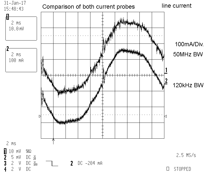
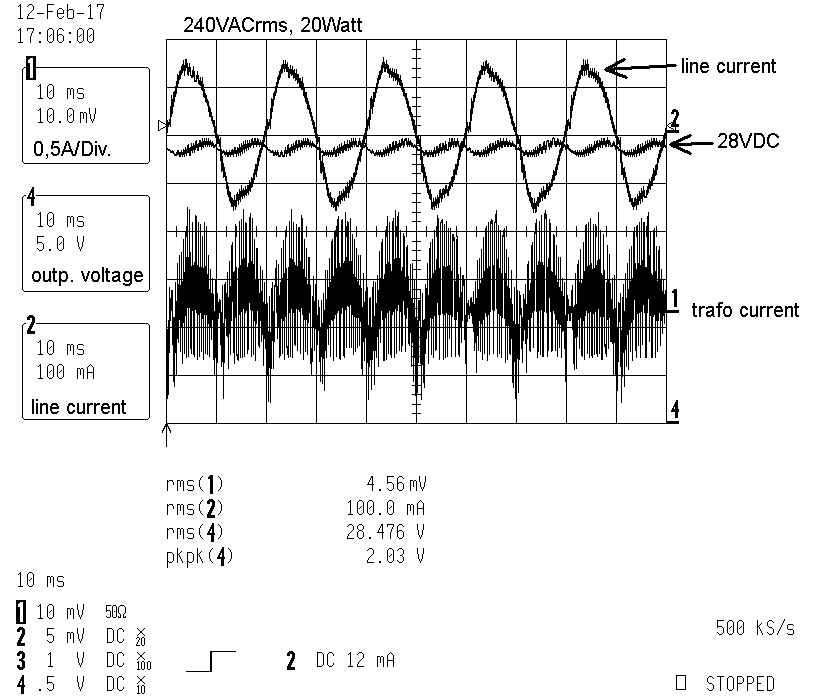
| Both current probes compared under the same line current. 50MHz probe shows a more noisy line current compared with the 120kHz probe, fundamental waveform looks similar. |
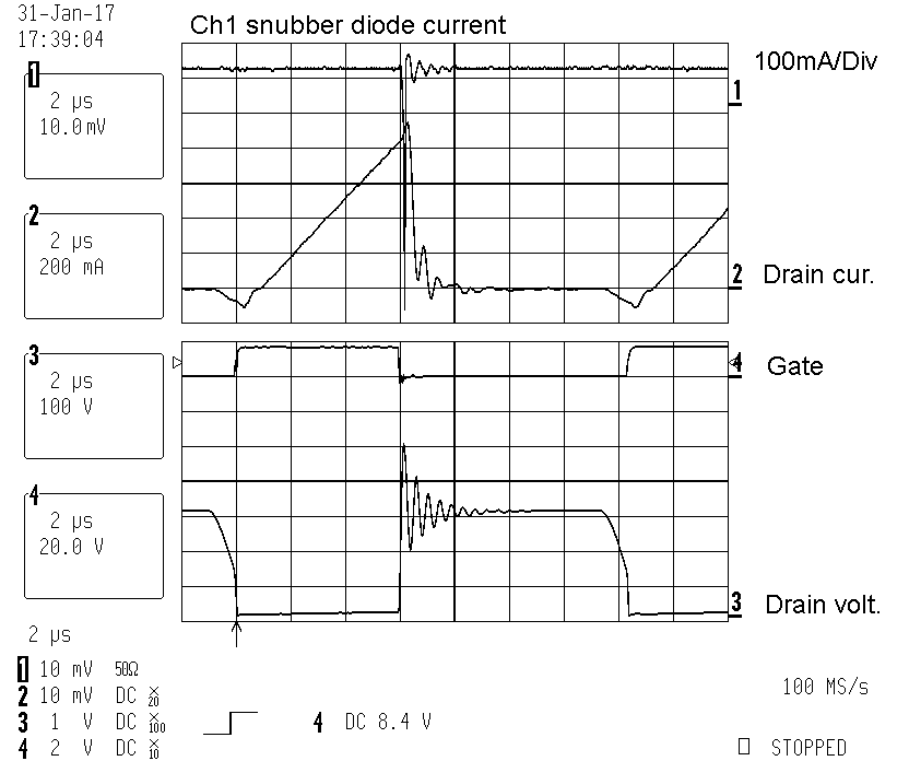
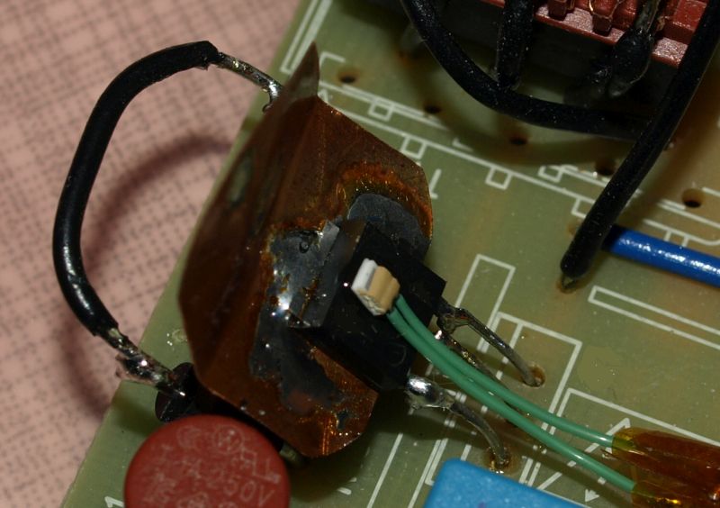
| Ch1 Snubber diode current on primary winding. MOSFET switching-OFF and snubber diode becomes conducting. |
|
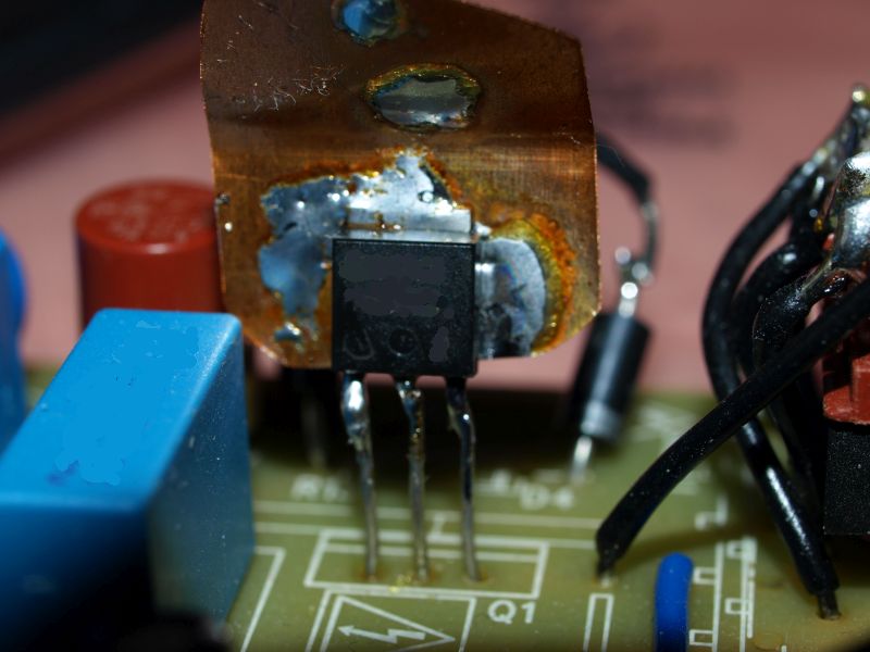
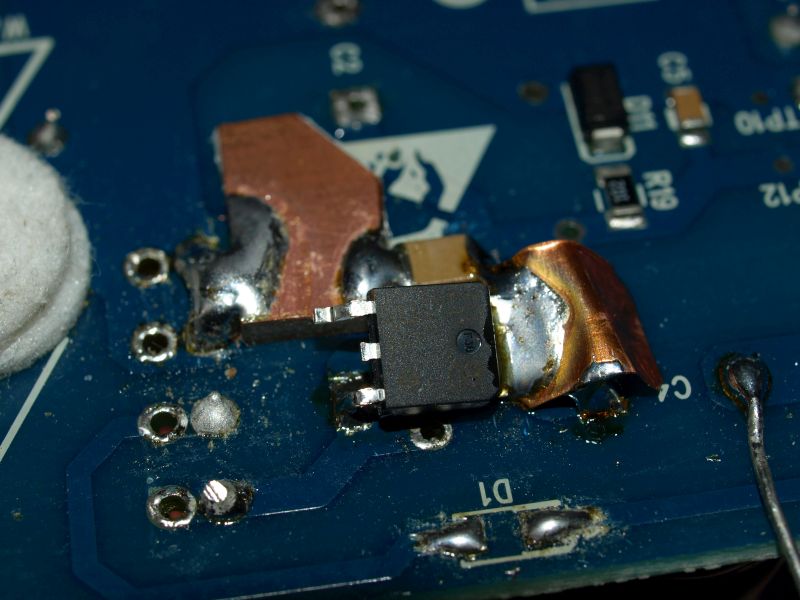
Copperfoil as heatsink, approximately same size on the later PCB.
Behind transistor the snubber diode network. Changing parts with
different package, always demanding. Here - no problem, but
some Evalboards
coming with 0402 resistor size, not nice, when changing many
times. Transformer changed before, changed orientation, longer wires are not good for EMC. A selfmade board is more flexible for changes. Small parts on a evaluation board, shows how small the PCB space can be, but difficult to change.
Most reasons for later series-errors: not tested enough. A selfmade copper PCB gives the designer an easy possibility to test all voltage and current nodes. In many cases designers have not enough test equipment in the labority. The saved money for missing equipment and extended tests - will be often payed later with design-errors in the field - ten times the costs of the equipment and the tests. Best developments methods consider these important issues:
Also for this project I can not fullfil these four items, would cost me too much time. In the past I did projects following exactly all four items, depends on the project value. |
|
Parts used now: MOSFET xxxxxxxx, 800V, 3.9A, 1400mOhm, 0,47€/1k Output Schottky Diode xxxxxxxxx, 100V, 5A, low-forward-voltage, 0,28€/1k Parts used before: MOSFET xxxxxxxxxxx, 800V, 4000mOhm, 0,33€/1k Silicon diode xxxxxxxxxxx, approx. 0,14€ to 0,20€ /1k Both parts a compromize of application, maximum ratings and lowest price. Former smaller MOSFET had 4000 mOhm (too much). Former xxxxxx silicon diode has >0.6V forward-voltage, a waste of thermal energy compared to the schottky diode. Improved parts prevent the PCB from extra heating-up. PCB has to run under approx. max. 55°C environmental temperature. |
|
PT1000 platinum resistor mounted on the MOSFET package, measured with a 34401A multimeter.
Placing the PT1000 direct on the Drain-Copper-Heatsink would measure the silicon temperature more precisely, but would be an unnecessary isolating risk - up to 700V drain voltage with additional >1MHz AC ringing. The PT1000 ceramic body must isolate this voltage (could do) to the DMM input, it´s safer mounting the PT1000 on the plastic. |
|
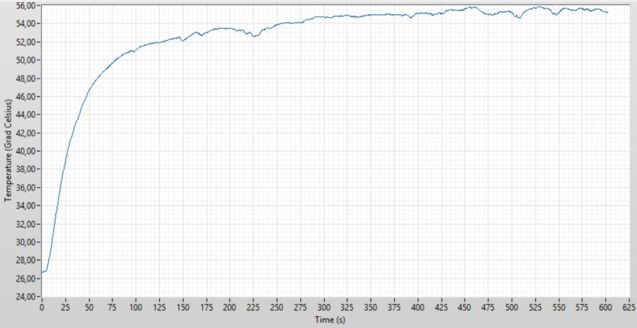
240VAC rms, load 20W, 28VDC
Power-ON ambient temperature 24°C (27°C comes from an not completely cooled-down PCB). After 600s the MOSFET package settles to 56°C, delta-temperature 32°C. Assuming 55°C ambient temperature, MOSFET package rise up to 87°C, perhaps 90°C in the silicon. The PCB will be enclosed in a box without convection, therefore an additional temperature rise, I guess at least 105°C final silicon temperature. It´s decision if the temperature rise can be accepted in the application. Highly recommended, layout with an improved thermal SMD heatsink into the copper planes, spreading heat into the PCB. Observe MOSFET temperatures with the necessary respect. |
|
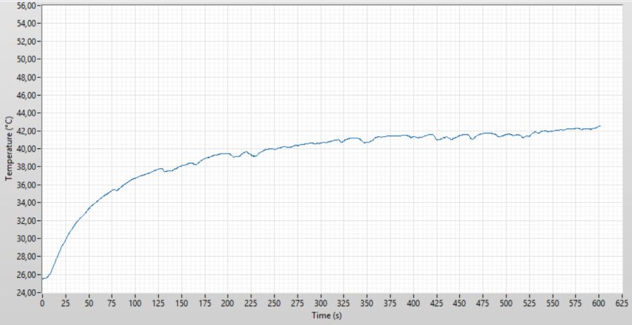
100VAC rms, load 20W, 28VDC
MOSFET runs cooler, this means switching losses of the MOSFET increase with higher line voltages. MOSFET conduction losses are not high. Temperature is not short-time-constant, heatsink is under free moving air. Heatsink is part of the control loop, power in the transistor is propably not short-time-constant. Line rms voltage short-time-constant? |
|
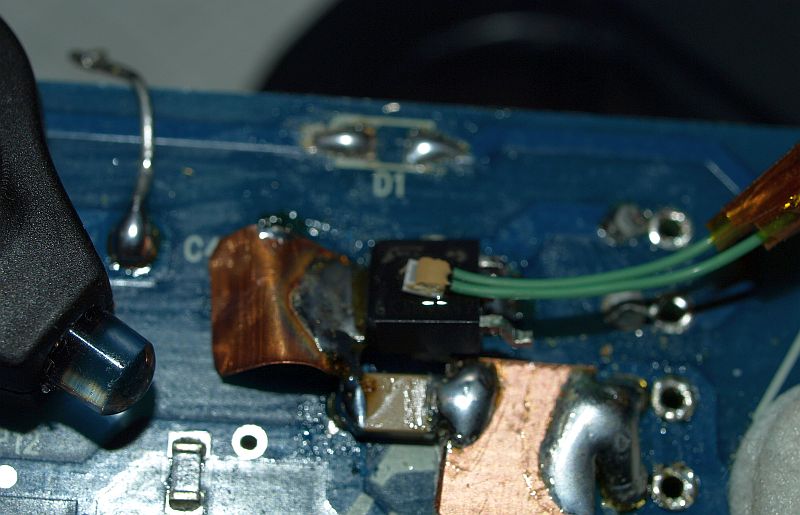
PT1000 platinum resistor mounted on the output rectifier schottky diode.
PT1000 glued with an ultraviolett light glue. On the left side there is the ultraviolett LED. It is a comfortable glue for this purpose, easy to handle, takes only 3 seconds of direct UV light. PT1000 can be easily removed with a sharp knife. |
|
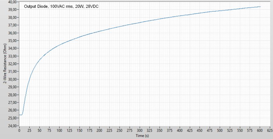
Output
Rectifier Schottky Diode, line 100VACrms, 20W, 28VDC.
Approximately 15°C
temperature rise - no problem.
Very clean noiseless response, not much moving air under
the PCB. Secondary side power is constant due control loop.
|
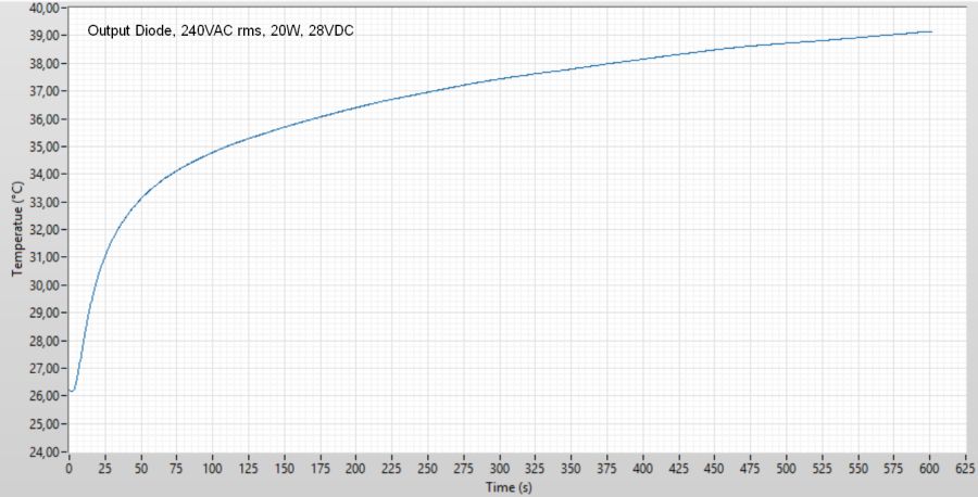
| Output Rectifier Schottky Diode Heat-Up under line 240VACrms, 20W, 28VDC - same as with 100VACrms. |
|
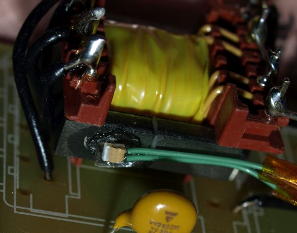
PT1000 platinum resistor on the transformer core.
|
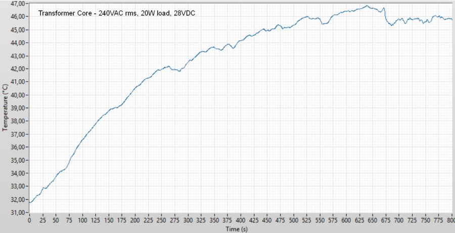
| Transformer core under line 240VACrms, 20Watt load, 28VDC.
Core temperature approx. 46°C - no problem. Core temperature should remain always within datasheet recommendations, if too much, core inductance decrease, resulting in fast rising and too high coil currents, can damaging the MOSFET or controller IC becomes an over-current-detection status. Very high core temperatures can damage the galvanic isolation of the coil, resulting in an insulating safety error - dangerous error condition for users life. High core temperature could also accelerate ageing of isolation material, difficult to predict - too much heat, avoid. All windings should be always tested for permanent overload and short-cut condition. Check if controller IC detects:
Especially auxilliary windings which are not directly power controlled by the controller IC, they can cause dangerous overlaod situations. A winding with uncontrolled power can run hot and can destroy the winding-insulation --- undetectable overpower situation for a single winding. Core becomes hot only under too much overall-power, core don´t know which winding caused the heat. A single overloaded auxiliary winding can become hot if the power in this winding can not be limited by the controller. Core can remain cold under a single winding overload, it is a winding overheating only ---- |
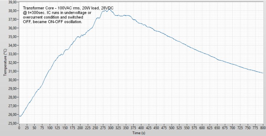
| Temperature rise under 100VAC rms, lowest
possible line voltage under 20W and 28VDC. At t=300s core heated up, changed current conditions detected by IC, resulting in switching OFF the circuit. Measurement must be done again with a little higher line voltage. This measurement is a very good example why circuits always have to be tested ON or better OVER their limits. Testing OVER the specified operating range shows weak points. Remember the four points testing method: 4.) fully tested outside the maximum operating conditions, search for HALT test failures. Figure 46 it is a wonderful example for item 4.) - Test outside the specified operating range, for example if 90VACrms are specified, test for example at 70VACrms - search for the UNKNOWN ERRORS. Force the circuit into errors. The kind of error will show you the next weak point in the full error chain. Here in this case, the overcurrent detection should be increased or the maximum load reduced. After detecting and understanding the error, the stoping error should be removed by a circuit change or the test should be forced to continue (by external circuit operations) until to the next stoping error occurs. Figure 46 shows the basic idea behind an HALT test. When testing below or exactly up to the specified borders, the error can never be detected. Designer thinks everything is OK, but a weak design-issue can exist under field-conditions. Propably already 10000 units selled on the market before recognizing the weak design-issue. Even when the field will never brings up an undetected error, a continued forced HALT test shows many weak point in the circuit. HALT testing is a powerful method for testing electronics and special for detecting weak design-issues. Unfortunately professional HALT testing is time demanding and requires expensive climate chambers with fast changing temperatures, HALT testing requires experience and preparation. The tests done with this power supply are only a "scratching the surface" in the world of professional HALT tests. Interested readers should read books about this method. Remember also this: "the saved money for missing test equipment and extended tests - will be often payed later with design-errors in the field - ten times the costs of the equipment and the tests." Über diese Punkte läßt sich lange diskutieren, es ist schwer deren Notwendigkeit sofort aus dem Stehgreif heraus zu beweisen. Länger als 10 Minuten sollte man nicht versuchen zu diskutieren, wer es dann nicht verstanden hat oder verstehen will, der versteht es auch nach 5 Stunden nicht. In solchen nicht mehr überzeugbaren Situationen zählt der Eigenschutz des Entwicklers - ruhig bleiben und Recht geben. Man muss andere nicht zu ihrem Glück zwingen. Das technische Verständnis zu erlangen ist der leichteste Teil für den Ingenieur, manche Dämlichkeiten zu ertragen der weitaus schwierigere Teil. |
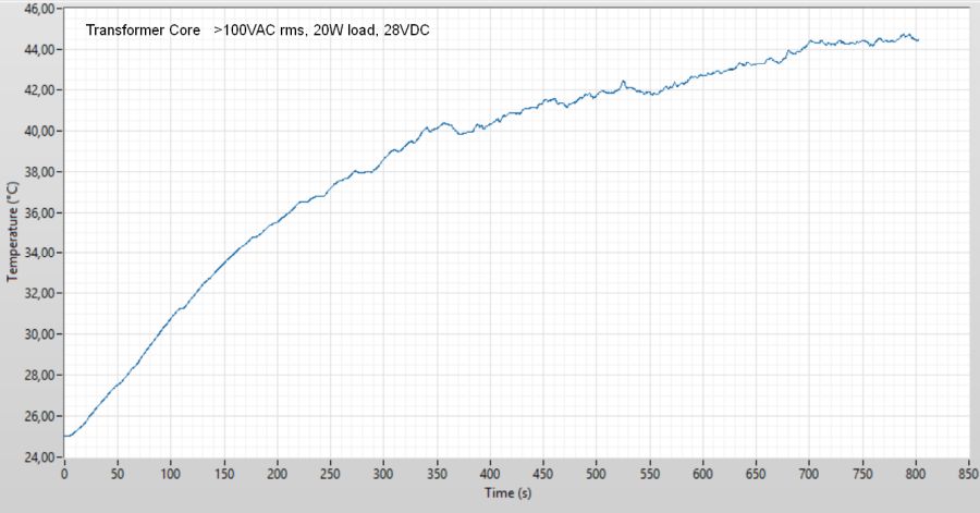
| Transformer core under line >100VAC rms, 20Watt, 28VDC, 45°C - no problem. |
|
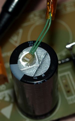
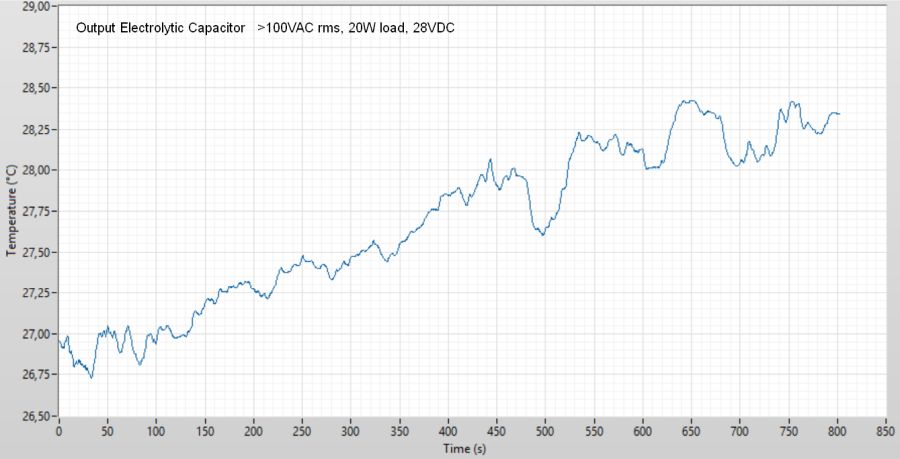
PT1000 platinum resistor, output electrolytic capacitor.
|
|
Output capacitor 2200µF/50V, >100VACrms, 20Watt, 28VDC, 29°C - no problem.
This capacitor will have a long life. |
|
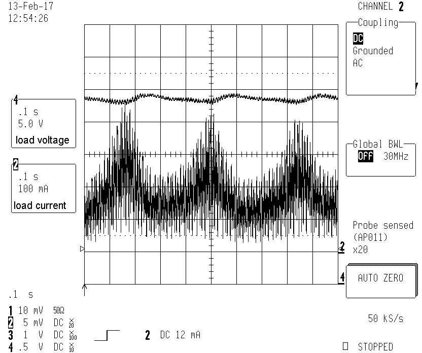
Testing the power supply with a typical load used in the application.
Load operates and starts clean from 60VAC rms up to 275VAC rms (rms voltage measured with 34401A, 275V highest tested voltage). This world-wide power supply input works fine. At the beginning of the development start with a ohmic load, after the circuit becomes stable begin testing with a application load. |
 .
.