|
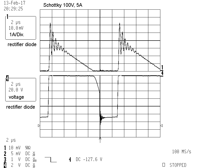
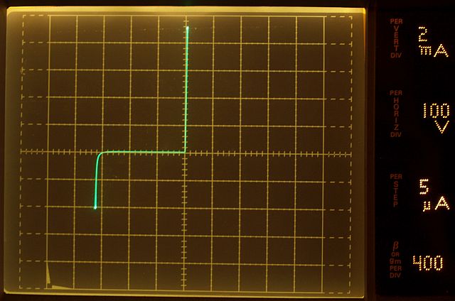
100V, 5A Schottky Diode
Curve Tracer show four quadrants. Diode starts conducting at -130 volt.
|
|
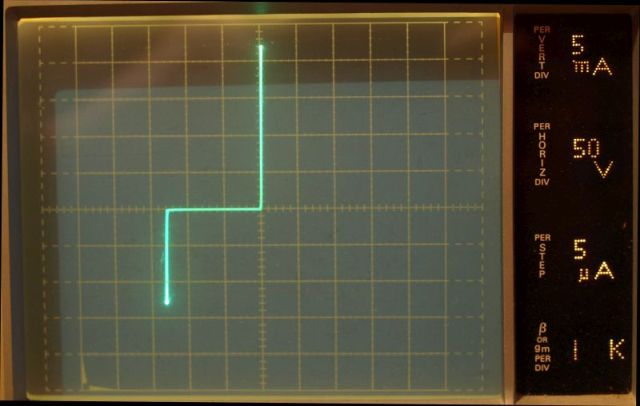
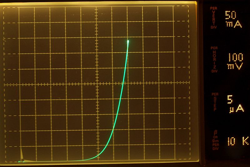
100V, 5A Schottky Diode
Curve Tracer shows first quadrant.100mA @ 400mV 400mA @ 450mV |
| 240VAC
rms, load 20W, 28VDC - 100V/5A schottky diode can not be used -
reverse voltage is too low, reverse voltage reach conducting area. Must be replaced by a higher voltage silicon diode. Up to 7A peak currents. |
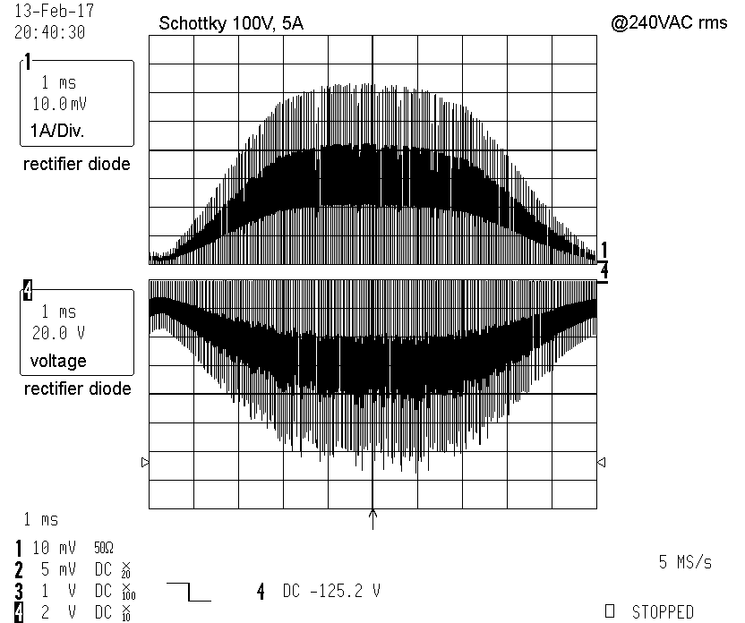
| 240VAC rms, 20W load, 28VDC - 100V 5A Schottky diode starts reverse conducting when reaching 240VAC rms. |
| silicon diode with 200V, 3A, 0.14€/1k Reverse Breakdown at 300V |
|
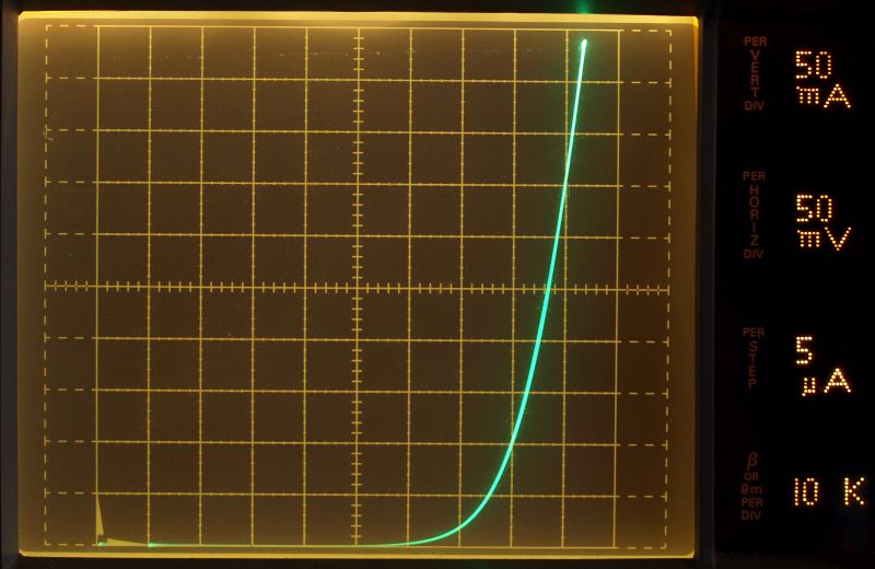
silicon diode with 200V, 3A
100mA @ 600mV
400mA @ 720mV |
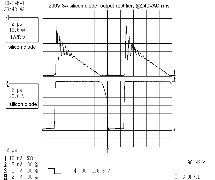
| Silicon diode (200V, 3A) @240VAC rms reach a reverse voltage -120V. Reverse voltage within the specified -200V. |
| Reverse
voltage diode example shows importance for observing always all
voltages and currents. Do it at least once ! I never thought such a
28VDC winding has to block a large -120V. The theory behind that fact
is simple, but when not thinking about it, problem still exists.
Discussing and review a design with other colleagues, hearing their
proposals is recommended. My thoughts were: with -100V of the Schottky, there is enough distance to the absolute maximum rating. My thinking was wrong, because of not fully understanding this part of the circuit. When not 100% thinking about the theory => Testing is a must. Without doing this simple diode measurement such a weak design-issue could go into field. This diode issue is a typical design-error, nobody would ever find it on a production or end test. This diode circuit would run in the field without problems. But the day will come and there is one unit with a diode less than -120V combined with an temperature or line voltage extreme, the diode start reverse conducting and run in a thermal runaway - damage. When following the four methods, such an design-error can not happen. (taken from Part 2): "Best developments methods consider these important issues:
Point 3.) force the designer to measure the diode voltage and current waveform - designer would find error fast. Point 4.) if the designer forget to measure or don`t understand the measured diode waveforms, the extended test could brute force this Unknown Error. For e.g. when testing with a rising-up line voltage, may be at 300VAC rms - BÄNG and SMOKE -. Extended test force the designer to explain why the diode has damaged in this test. Designer wants to know why the diode damages, find it and explain. Also observe full circuit with a thermal camera, may be the diode is still cold at 290VAC rms, run fast hot under e.g. 295VAC rms - this is a stop signal for the test to find the reason first. For example if the AC line varistor blows first at 280VAC rms - don´t stop the extended test! Remove the AC line varistor, renew the melting fuse and continue testing, increase line voltage further until next Unknown Error occurs, in our case the blowing diode. Designer must explain the Unknown Errors - for the line varistor, easy to explain, varistor does the wanted overvoltage protection job. For the unknown diode error, after finding the reason (sometimes hard), designer make a big AHA ! In my experience, designers will change their design fast as possible within next days. Prevents from producing e.g. 10000 weak units, prevents from producing future 5*10000 weak units, because designers often copy their old design together with the unknown errors into the new design. Point 1.) helps the designer to do fast and reliable measurements. Point 2.) will document all happened issues. The circuit topology and concept is the most important key to the design success - but topology was not the topic of this application note - Purpose was showing measurements and development methods. |
 .
.